TL D 10044
NM93CS06LCS46LCS56LCS66L
256-1024-2048-4096-Bit
Serial
EEPROM
with
Extended
Voltage
(27V
to
55V)
and
Data
Protect
(MICROWIRE
Bus
Interface)
August 1996
NM93CS06L CS46L CS56L CS66L
256- 1024- 2048- 4096-Bit Serial EEPROM
with Extended Voltage (2 7V to 5 5V) and Data Protect
(MICROWIRE
TM
Bus Interface)
General Description
The
NM93CS06L CS46L CS56L CS66L
devices
are
256 1024 2048 4096 bits
respectively
of non-volatile
electrically erasable memory divided into 16 64 128 256 x
16-bit registers (addresses) The NM93CSxxL Family func-
tions in an extended voltage operating range and is fabri-
cated using National Semiconductor's floating gate CMOS
technology for high reliability high endurance and low pow-
er consumption N registers (N
s
16 N
s
64 N
s
128 N
s
256) can be protected against data modification by pro-
gramming the Protect Register with the address of the first
register to be protected against data modification (All regis-
ters greater than or equal to the selected address are then
protected from further change ) Additionally this address
can be ``locked'' into the device making all future attempts
to change data impossible
These devices are available in both SO and TSSOP pack-
ages for small space considerations
The serial interface that controls these EEPROMs is
MICROWIRE compatible providing simple interfacing to
standard microcontrollers and microprocessors
There
are a total of 10 instructions 5 which operate on the EEPROM
memory and 5 which operate on the Protect Register The
memory instructions are READ
WRITE
WRITE ALL
WRITE ENABLE and WRITE DISABLE The Protect regis-
ter
instructions
are
PRREAD
PRWRITE
PRCLEAR
PRDISABLE and PRENABLE
Features
Y
Sequential register read
Y
Write protection in a user defined section of memory
Y
2 7V to 5 5V operating range in all modes
Y
Typical active current of 200 mA typical standby
current of 1 mA
Y
No erase required before write
Y
Reliable CMOS floating gate technology
Y
MICROWIRE compatible serial I O
Y
Self timed write cycle
Y
Device status during programming mode
Y
40 year data retention
Y
Endurance 10
6
data changes
Y
Packages Available
8-pin SO
8-pin DIP
and 8-pin
TSSOP
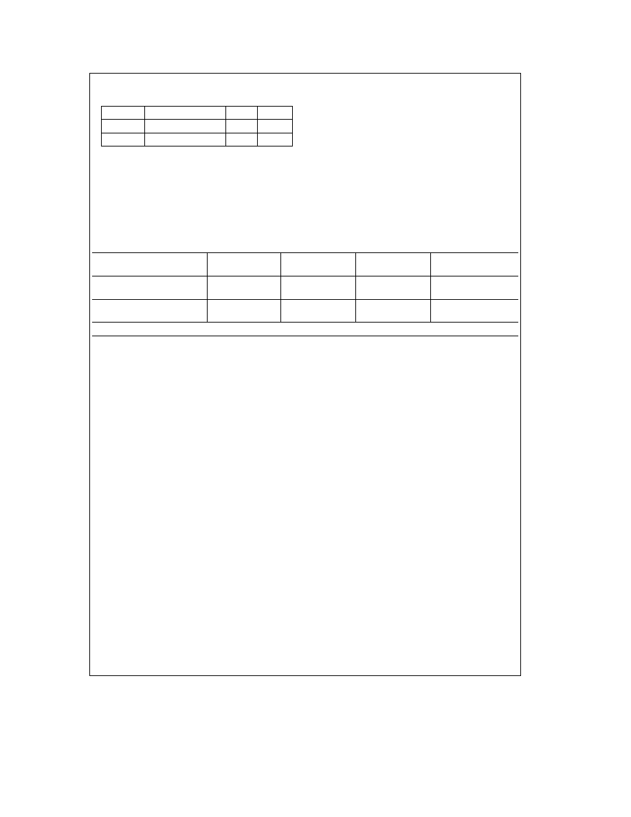
Block Diagram
TL D 10044 � 1
TRI-STATE
is a registered trademark of National Semiconductor Corporation
MICROWIRE
TM
is a trademark of National Semiconductor Corporation
C1996 National Semiconductor Corporation
RRD-B30M126 Printed in U S A
http
www national com
Connection Diagrams
Dual-In-Line Package (N)
8-Pin SO Package (M8) and 8-Pin TSSOP Package (MT8)
TL D 10044 � 2
Top View
See NS Package Number N08E (N)
See NS Package Number M08A (M8)
See NS Package Number MTC08 (MT8)
Pin Names
CS
Chip Select
SK
Serial Data Clock
DI
Serial Data Input
DO
Serial Data Output
GND
Ground
PE
Program Enable
PRE
Protect Register Enable
V
CC
Power Supply
Ordering Information
Commercial Temp Range (0 C to
a
70 C)
Order Number
NM93CS06LN NM93CS46LN NM93CS56LN NM93CS66LN
NM93CS06LM8 NM93CS46LM8 NM93CS56LM8 NM93CS66LM8
NM93CS46LMT8 NM93CS56LMT8 NM93CS66LMT8
Extended Temp Range (
b
40 C to
a
85 C)
Order Number
NM93CS06LEN NM93CS46LEN NM93CS56LEN NM93CS66LEN
NM93CS06LEM8 NM93CS46LEM8 NM93CS56LEM8 NM93CS66LEM8
NM93CS46LEMT8 NM93CS56LEMT8 NM93CS66LEMT8
Automotive Temp Range (
b
40 C to
a
125 C)
Order Number
NM93CS06LVN NM93CS46LVN NM93CS56LVN NM93CS66LVN
NM93CS06LVM8 NM93CS46LVM8 NM93CS56LVM8 NM93CS66LVM8
NM93CS46LVMT8 NM93CS56LVMT8 NM93CS66LVMT8
http
www national com
2
Absolute Maximum Ratings
(Note 1)
If Military Aerospace specified devices are required
please contact the National Semiconductor Sales
Office Distributors for availability and specifications
Ambient Storage Temperature
b
65 C to
a
150 C
All Input or Output Voltages
a
6 5V to
b
0 3V
with Respect to Ground
Lead Temperature (Soldering 10 sec )
a
300 C
ESD rating
2000V
Operating Conditions
Ambient Operating Temperature
NM93CSxxL
0 C to
a
70 C
NM93CSxxLE
b
40 C to
a
85 C
Power Supply (V
CC
) Range
Read Mode
2 0V to 5 5V
WRALL Bulk Programming
3 0V to 5 5V
All Other Modes
2 5V to 5 5V
DC and AC Electrical Characteristics 2V
k
V
CC
k
4 5V
Symbol
Parameter
Conditions
Min
Max
Units
I
CCA
Operating Current
CS
e
V
IH
SK
e
250 kHz
1
mA
I
CCS
Standby Current
CS
e
V
IL
50
m
A
I
IL
Input Leakage
V
IN
e
0V to V
CC
g
1
m
A
I
OL
Output Leakage
(Note 4)
V
IL
Input Low Voltage
b
0 1
0 15 V
CC
V
V
IH
Input High Voltage
0 8 V
CC
V
CC
a
1
V
OL
Output Low Voltage
I
OL
e
10 mA
0 1 V
CC
V
V
OH
Output High Voltage
I
OH
e b
10 mA
0 9 V
CC
f
SK
SK Clock Frequency
(Note 5)
0
250
kHz
t
SKH
SK High Time
1
m
s
t
SKL
SK Low Time
1
m
s
t
SKS
SK Setup Time
SK must be at V
IL
for
0 2
m
s
t
SKS
before CS goes high
t
CS
Minimum CS
(Note 2)
1
m
s
Low Time
t
CSS
CS Setup Time
0 2
m
s
t
PRES
PRE Setup Time
0 2
m
s
t
PES
PE Setup Time
0 2
m
s
t
DIS
DI Setup Time
0 4
m
s
t
DH
DO Hold Time
70
ns
t
CSH
CS Hold Time
0
m
s
t
PEH
PE Hold Time
0 4
m
s
t
PREH
PRE Hold Time
0 4
m
s
t
DIH
DI Hold Time
0 4
m
s
t
PD1
Output Delay to ``1''
2
m
s
t
PD0
Output Delay to ``0''
2
m
s
t
SV
CS to Status Valid
1
m
s
t
DF
CS to DO in
CS
e
V
IL
0 4
m
s
TRI-STATE
t
WP
Write Cycle Time
15
ms
http
www national com
3
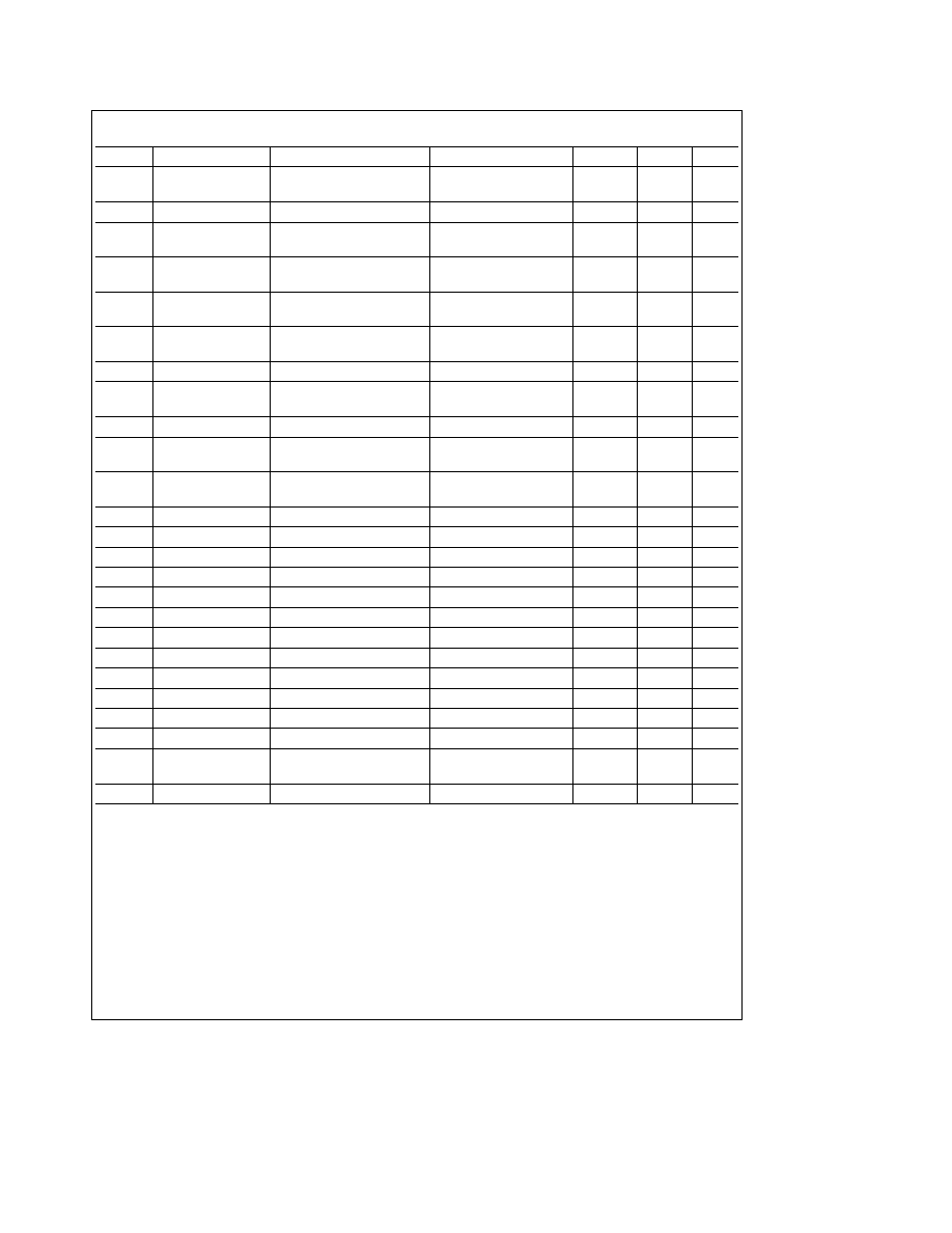
DC and AC Electrical Characteristics 4 5V
k
V
CC
k
5 5V
Symbol
Parameter
Part Number
Conditions
Min
Max
Units
I
CCA
Operating Current
CS
e
V
IH
SK
e
1 0 MHz
1
mA
CMOS Input Levels
I
CCS
Standby Current
CS
e
V
IL
50
m
A
I
IL
Input Leakage
V
IN
e
0V to V
CC
g
1
m
A
I
OL
Output Leakage
(Note 4)
V
IL
Input Low Voltage
b
0 1
0 8
V
V
IH
Input High Voltage
2
V
CC
a
1
V
OL1
Output Low Voltage
I
OL
e
2 1 mA
0 4
V
V
OH1
Output High Voltage
I
OL
e
400 mA
2 4V
V
OL2
Output Low Voltage
I
OL
e
10 mA
0 2
V
V
OH2
Output High Voltage
I
OL
e b
10 mA
V
CC
b
0 2
f
SK
SK Clock Frequency
(Note 5)
0
1
MHz
t
SKH
SK High Time
NM93CS06L-NM93CS66L
250
ns
NM93CS06LE-NM93CS66LE
300
t
SKL
SK Low Time
250
ns
t
SKS
SK Setup Time
SK must be at V
IL
for
50
ns
t
SKS
before CS goes High
t
CS
Minimum CS
(Note 2)
250
ns
Low Time
t
CSS
CS Setup Time
50
ns
t
PRES
PRE Setup Time
50
ns
t
DH
DO Hold Time
70
ns
t
PES
PE Setup Time
50
ns
t
DIS
DI Setup Time
100
ns
t
CSH
CS Hold Time
0
ns
t
PEH
PE Hold Time
250
ns
t
PREH
PRE Hold Time
50
ns
t
DIH
DI Hold Time
20
ns
t
PD1
Output Delay to ``1''
500
ns
t
PD0
Output Delay to ``0''
500
ns
t
SV
CS to Status Valid
500
ns
t
DF
CS to DO in
CS
e
V
IL
100
ns
TRI-STATE
t
WP
Write Cycle Time
10
ms
http
www national com
4
Capacitance
(Note 3)
T
A
e
25 C f
e
1 MHz
Symbol
Test
Max
Units
C
OUT
Output Capacitance
5
pF
C
IN
Input Capacitance
5
pF
Note 1
Stress ratings above those listed under ``Absolute Maximum Ratings'' may cause permanent damage to the device This is a stress rating only and
operation of the device at these or any other conditions above those indicated in the operational sections of the specification is not implied Exposure to absolute
maximum rating conditions for extended periods may affect device reliability
Note 2
CS (Chip Select) must be brought low (to V
IL
) for an interval of t
CS
in order to reset all internal device registers (device reset) prior to beginning another
opcode cycle (This is shown in the opcode diagrams in the following pages)
Note 3
This parameter is periodically sampled and not 100% tested
Note 4
Typical leakage values are in the 20 nA range
Note 5
The shortest allowable SK clock period
e
1 f
SK
(as shown under the f
SK
parameter) Maximum SK clock speed (minimum SK period) is determined by the
interaction of several AC parameters stated in the datasheet Within this SK period both t
SKH
and t
SKL
limits must be observed Therefore it is not allowable to set
1 f
SK
e
t
SKH (minimum)
a
t
SKL (minimum)
for shorter SK cycle time operation
AC Test Conditions
V
CC
Range
V
IL
V
IH
V
IL
V
IH
V
OL
V
OH
I
OL
I
OH
Input Levels
Timing Level
Timing Level
2 0V
s
V
CC
k
4 5V
0 3V 1 8V
1 0V
0 8V 1 5V
g
10 mA
(Extended Voltage Levels)
4 5V
s
V
CC
s
5 5V
0 4V 2 4V
1 0V 2 0V
0 4V 2 4V
b
2 1 mA 0 4 mA
(TTL Levels)
Output Load 1 TTL Gate (C
L
e
100 pF)
http
www national com
5