
TL D 12302
NM95HS01NM95HS02
HiSeC
High
Security
Rolling
Code
Generator
February 1996
NM95HS01 NM95HS02
HiSeC
TM
High Security Rolling Code Generator
General Description
The NM95HS01 02 HiSeC Rolling Code Generator is a
small footprint monolithic CMOS device designed to pro-
vide a complete low-cost high security solution to the prob-
lem of generating encrypted signals for remote keyless en-
try (RKE) applications
The NM95HS01 02 generates a fully encoded bit stream
each time one of (up to) 4 switch inputs is activated The
patented
coding scheme utilizes 2
48
possible user-pro-
grammable coding combinations and features high linear
complexity and correlation immunity High security is guar-
anteed by generating a unique (rolling) code for each trans-
mission and can be further enhanced by creating custom-
ized algorithms for individual customers With this product
each key can be designed to be both unique and highly
secure
The NM95HS01 02 supports either an IR or RF signal
transmitter and can be clocked with either an RC clock
(NM95HS01) or a crystal oscillator (NM95HS02) The de-
vice operates over a voltage range of 2 2V to 6 5V and
offers a low power standby mode (
k
1 mA) for battery appli-
cations The product is available in both 8-pin and 14-pin SO
packages with 2 or 4 key switch inputs that can be used for
customer presets such as seat positions and vehicle oper-
ating functions such as car door locking unlocking
Patents Pending
Features
Y
High security coding scheme with 2
48
combinations
Y
High linear complexity and correlation immunity
Y
2 2V to 6 5V operation
Y
Less than 1 mA standby current
Y
Full resynchronization capability
Y
Unique customized algorithm option
Y
13 bytes on-chip non-volatile configuration memory
Y
RC or XTAL clock options for to 4 1 MHz operation
Y
Supports both IR and RF signal transmission
Y
Selection of bit coding and transmission frame formats
Y
Space saving narrow body SO8 or SO14 packages
Y
Up to 4 key switch inputs on SO14 package
Applications
Y
Remote Keyless Entry (RKE) applications
Y
Burglar alarms garage door openers
Y
Individualized recognition transmission systems
Y
Personalized consumer automotive applications
Relevant Documents
Y
MM57HS01 datasheet
Y
Designing and Programming a Complete HiSeC
TM
-
based RKE System
AN-985
Y
HiSeC Remote Keyless Entry Solution Encoder Decod-
er Chip Set User's Manual
AN-355
Functional Block Diagram
TL D 12302 ≠ 1
Note
Signals shown are internal logic signals
FIGURE 1
HiSeC
TM
and MICROWIRE
TM
are trademarks of National Semiconductor Corporation
C1996 National Semiconductor Corporation
RRD-B30M66 Printed in U S A

General Characteristics
The NM95HS01 02HiSeC Generator was developed to
meet existing standards for rolling code-based security sys-
tems
Theft prevention systems typically involve user identification
and transmission of information at various distances from
the vehicle These Remote Keyless Entry (RKE) systems
are generally implemented with IR transmitters for short dis-
tances or RF transmitters for longer distances RF trans-
mission has become state of the art however the longer
distances involved require a much higher degree of security
since the possibility of signal interception is greatly in-
creased
These
applications
are
ideally
served
by
the
NM95HS01 02 This generator is a small footprint low cur-
rent solution that supports both IR and RF transmission
The device is available in an 8-pin SO package with 2 key
switch inputs or a 14-pin SO package with 4 key switch
inputs
The proprietary coding scheme used generates a rolling
code based on 2
48
possible user combinations and en-
sures a high level of coding security for any RKE applica-
tion The NM95HS01 can be clocked with an RC circuit
while the NM95HS02 can be clocked with a crystal oscilla-
tor
General Device Operation
The Functional Block Diagram
(Figure 1) shows the internal
elements of the code generating logic and program regis-
ters
The NM95HS01 02 HiSeC Generator achieves its high se-
curity level by combining the contents of several dynamic
data registers in a non-linear manner to generate an encod-
ed output Data in the registers is comprised of a mixture of
user programmable data factory programmable data and
randomized data This inherently random and separate data
is encrypted by clocking it through a non-linear logic block
and feeding part of the output back to produce a final coded
output with a high degree of linear complexity and correla-
tion immunity
The NM95HS01 02 incorporates 13 bytes of non-volatile
EEPROM memory which can be used to configure the de-
vice registers This memory is accessible to the user and
can be configured to the desired configuration then write-
disabled to prevent tampering
User programmable data includes 24 bits of the code block
a 24-bit key ID register and an 8-bit sync field register
The 24-bit key ID register can be used to configure a large
number of unique keys each of which will produce a unique
encoded output bit stream The 24 bits in the code genera-
tor block are mixed with coded data
The output of this block is then fed into the 24- 36-bit buffer
register where the 40 bits are recombined to produce a 24-
or 36-bit output (a user option) The 8-bit sync field register
can be configured by the user to provide a pattern to facili-
tate synchronization between the transmitter and receiver
The details of the code block are available to customers
and exclusive algorithms are available and under contract
with National Call your local sales office for details
The HiSeC Generator is shipped with a standard algorithm
as a standard product with the configuration shown
Figure 2 shows a general operational block diagram of the
NM95HS01 02 HiSeC Generator The 4 key switch inputs
shown use internal pull-up resistors and are suitable for
normally open single pole input switches connected to
ground The inputs are buffered by debounce logic which
repeatedly polls the inputs to determine if a key switch has
been asserted If any key switch input is seen as low for four
continuous 10 ms samples its associated output is set high
the HiSeC control logic is activated and a security code is
generated and transmitted
The timer block is used to set the key debounce time and
the IR or RF clock times These clock times are used as the
time base for the chosen bit coding format The timer block
is also used to generate the interframe pause time and the
timeout delay if these are enabled These parameters are
configured by the user in the 13-byte on-chip EEPROM ar-
ray
The NM95HS01 version of the device uses an RC network
to clock the CKI input pin The CKO LED pin is not required
for clocking but may be used for a visual indicator LED If
the NM95HS02 crystal oscillator version is used the device
is clocked using both the CKI and CKO pins If an LED is
used with this device it may be grounded through the
RFEN LED pin Either the CKO LED or the RFEN LED out-
put pins can provide the sink current needed to drive an
indicator LED The RFEN pin is active low during signal
transmission and is used to provide power to the RF circuit
only during transmission to increase battery life
The transmit output (TX) pin is a configurable logic level
output and is used to transmit the encoded bit stream An
on-chip power-on reset circuit is used to initialize the device
during power-up
http
www national com
2
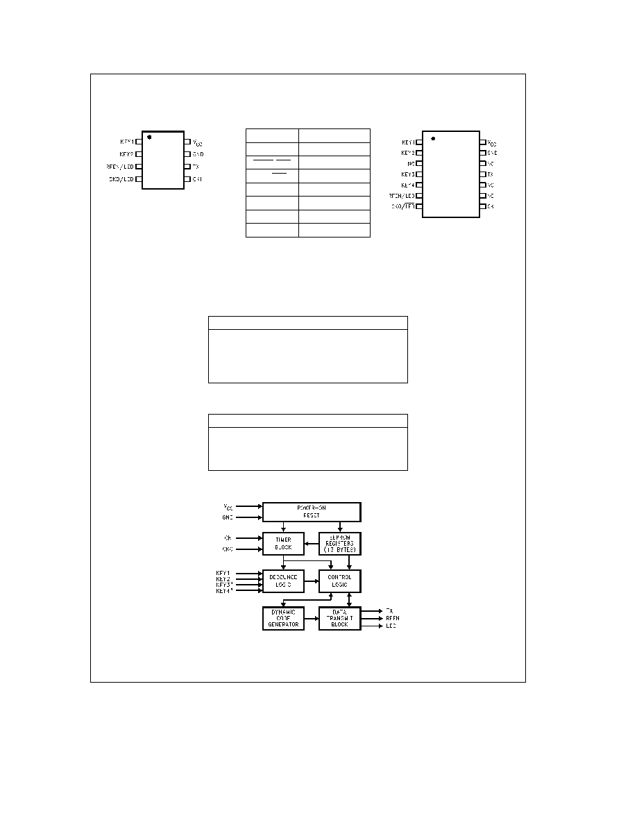
Connection Diagrams
8-Pin SO Package (M8)
TL D 12302 ≠ 4
Top View
See NS Package Number
M08A (M8) or N08E (N)
Pin Names
Pin
Description
KEYn
Key Input
RFEN LED
RF Enable LED
CKO LED
XTAL Clock LED
TX
Data Transmit
CKI
RC Clock Input
GND
Ground
V
CC
Supply Voltage
14-Pin SO Package (M14) and
14-Pin Dual-In-Line Package (N14)
14-Pin TSSOP Package (MT14)
TL D 12302 ≠ 5
Top View
See NS Package Number
M14A (M) MTC14 (MT14)
or N14A (N14)
Ordering Information
Commercial Temperature Range (0 C to
a
70 C)
Order Number
NM95HS01M8 NM95HS02M8
NM95HS01N NM95HS02N
NM95HS01M NM95HS02M
NM95HS01MT14 NM95HS02MT14
NM95HS01N14 NM95HS02N14
Extended Temperature Range (
b
40 C to
a
85 C)
Order Number
NM95HS01EM8 NM95HS02EM8
NM95HS01EN NM95HS02EN
NM95HS01EM NM95HS02EM
NM95HS01EN14 NM95HS02EN14
TL D 12302 ≠ 2
Note
Keys 3 and 4 available in 14-pin packages
FlGURE 2 Operational Block Diagram of the NM95HS01 02 HiSeC Generator
http
www national com
3
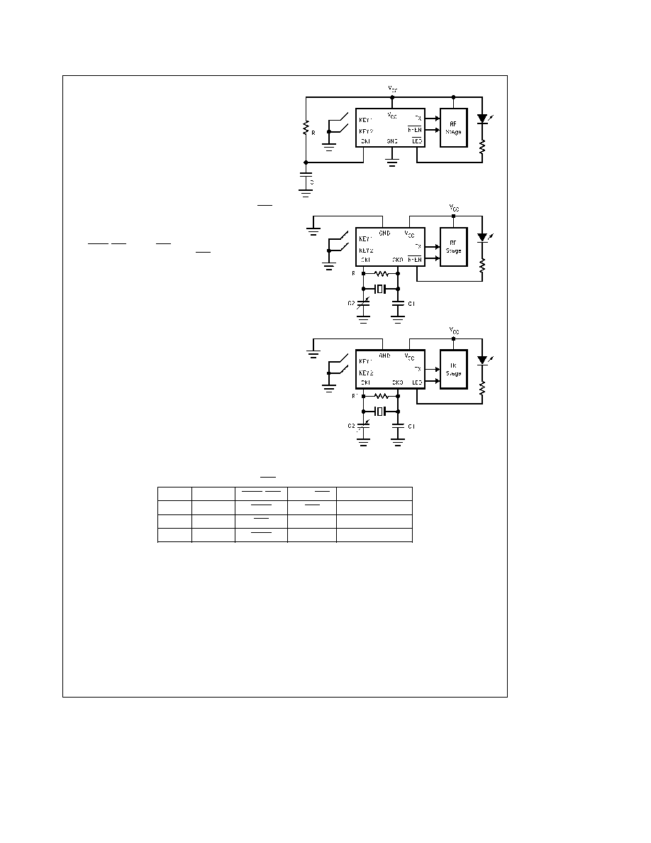
General Transmitter Circuit
Configurations
Figure 3 shows several typical circuit configurations for a
HiSeC based RKE system transmitter Note that all circuits
require few external components beyond a battery and
transmitter stage IR and RF bit timing may be optimized
through the timer block settings in the EEPR0M array which
allows flexibility in selecting the smallest and least expen-
sive clock components in the chosen design range
The first two circuits are examples of RF transmitter applica-
tions with both RC and crystal (XTAL) oscillator clocks the
third circuit is an example of an IR transmitter application
Two circuits are configured for an LED Note that the LED
pin refers to a visual indicator LED and not the IR LED
which might be used in an IR transmitter circuit
The LEDSEL bit in the EEPROM array determines whether
the RFEN LED or CKO LED pins are dedicated to the LED
for a particular circuit configuration LED pin select options
are detailed in Table I
Design considerations for selecting and optimizing clock
component values are detailed in the Generator Clock De-
sign Parameters section
General Receiver Circuit
Configurations
The NM95HS01 02 HiSeC Generator with the standard
customer algorithm is matched to a companion part
the
MM57HS HiSeC Decoder For applications requiring more
extensive receiver design and decoder programming a
COPS8xxx NM93Cx6 package is recommended A com-
plete discussion of receiver oonfigurations and considera-
tions can be found in the National Semiconductor Applica-
tion Note
How to Design and Program a HiSeC RKE Re-
ceiver using an 8-Bit Microcontroller
TL D 12302 ≠ 3
FIGURE 3 Typical Transmitter Circuit Configurations
TABLE I LED Pin Select Options
Clock
LEDSEL
RFEN LED
CKO LED
Function
RC
X
RFEN
LED
RF Mode with LED
XTAL
0
LED
CKO
RF Mode w o LED
XTAL
1
RFEN
CKO
IR mode with LED
Either the LED or RFEN outputs of the NM95HS01 02 can be used to indicate device transmis-
sion The LED output is active during a pause whereas the RFEN output is active during frame
transmission
The IR Drive Current is 10 mA so an amplifier stage may be needed
http
www national com
4

Bit Coding Formats
The NM95HS01 02 HiSeC Generator supports eleven-bit
coding formats which may be used for IR and RF transmis-
sion Seven-bit formats are available for RF applications
and four are available for IR applications One-bit format is
reserved for future use
Bit coding formats are selected by configuring four bits in
the EEPROM array IRSEL PRSEL2 PRSEL1 and PRSEL0
Table II shows the possible bit coding options available
Each bit coding format has a distinction which may be ad-
vantageous for a particular application RF bit coding format
0 is the simplest bit coding scheme and data may be easily
recovered from a transmission by exclusive OR-ing the data
and clock stream Both RF bit coding formats 0 and 2 have
a DC level that is independent of the data
RF format 4 and the IR modes operate with a constant
transmission energy per message and RF coding formats
1 3 5 and 7 are pulse-width modulated (PWM) formats
which are relatively easy to decode RF coding format 7 has
a low duty cycle
The IR bit coding formats are modulated versions of RF
coding format 4 and are all suitable for IR applications The
duty cycle and number of pulses are variable among these
four to allow the user to fine tune the IR circuit power curve
IR bit coding formats all follow the same general pattern In
this mode a logic ``1'' is always two periods long and a ``0''
is always three periods long This may be an important con-
sideration when considering preamble and sync timing
Waveform diagrams for all available RF and IR bit transmis-
sion coding formats are shown below
TABLE II Transmission Bit Coding Options
IRSEL PRSEL2 PRSEL1 PRSEL0
Function
0
0
0
0
RF Bit Coding Format 0
0
0
0
1
RF Bit Coding Format 1
0
0
1
0
RF Bit Coding Format 2
0
0
1
1
RF Bit Coding Format 3
0
1
0
0
RF Bit Coding Format 4
0
1
0
1
RF Bit Coding Format 5
0
1
1
0
Reserved
0
1
1
1
RF Bit Coding Format 7
1
0
0
0
IR Bit Coding Format 1
1
0
0
1
IR Bit Coding Format 2
1
0
1
0
IR Bit Coding Format 3
1
0
1
1
IR Bit Coding Format 4
1
1
X
X
Reserved
Bit Transmission Coding Formats
RF Bit Coding Format 0 (Manchester Code)
TL D 12302 ≠ 6
RF Bit Coding Format 1 (33% 66%
End High)
TL D 12302 ≠ 7
RF Bit Coding Format 2 (50% Duty Cycle)
TL D 12302 ≠ 8
RF Bit Coding Format 3 (25% 50%
Start High)
TL D 12302 ≠ 9
RF Bit Coding Format 4 (IR Style)
TL D 12302 ≠ 10
RF Bit Coding Format 5 (33% 66%
Start High)
TL D 12302 ≠ 11
http
www national com
5