TL D 8827
NMC27C32B
32768-Bit
(4096
x
8
)
CMOS
EPROM
December 1996
NMC27C32B
32 768-Bit (4096 x 8) CMOS EPROM
General Description
The NMC27C32B is a 32k UV erasable and electrically re-
programmable CMOS EPROM ideally suited for applica-
tions where fast turnaround pattern experimentation and
low power consumption are important requirements
The NMC27C32B is designed to operate with a single
a
5V
power supply with
g
10% tolerance
The NMC27C32B is packaged in a 24-pin dual-in-line pack-
age with a quartz window The quartz window allows the
user to expose the chip to ultraviolet light to erase the bit
pattern A new pattern can then be written electrically into
the device by following the programming procedure
This EPROM is fabricated with National's proprietary time
proven CMOS double-poly silicon gate technology which
combines high performance and high density with low pow-
er consumption and excellent reliability
Features
Y
Low CMOS power consumption
Active Power 55 mW Max
Standby Power 0 55 mW Max
Y
Extended temperature range
b
40 C to
a
85 C
Y
Fast and reliable programming
Y
TTL CMOS compatible inputs outputs
Y
TRI-STATE
output
Y
Manufacturer's identification code for automatic
programming
Y
High current CMOS level output drivers
Y
Compatible with NMOS 2732
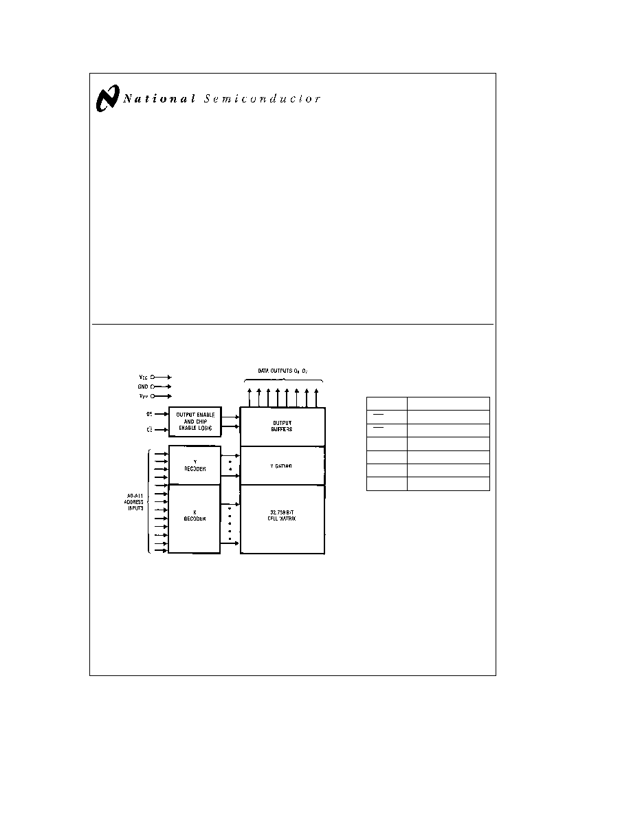
Block Diagram
TL D 8827 � 1
Pin Names
A0 � A11
Addresses
CE
Chip Enable
OE
Output Enable
V
PP
Programming Voltage
O
0
� O
7
Outputs
V
CC
Power Supply
GND
Ground
TRI-STATE
is a registered trademark of National Semiconductor Corporation
C1996 National Semiconductor Corporation
RRD-B30M17 Printed in U S A
http
www national com
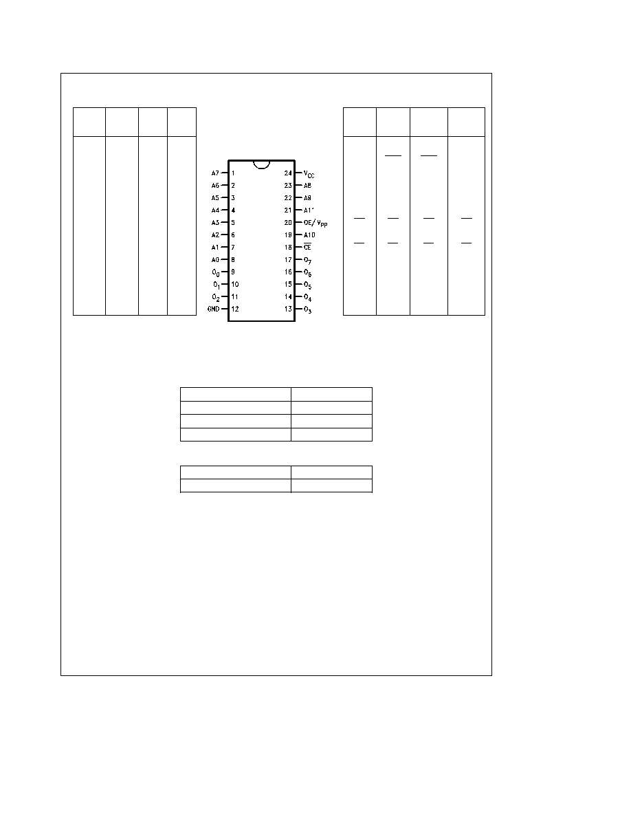
Connection Diagram
27C256
27C128
27C64
27C16
27256
27128
2764
2716
V
PP
V
PP
V
PP
A12
A12
A12
A7
A7
A7
A7
A6
A6
A6
A6
A5
A5
A5
A5
A4
A4
A4
A4
A3
A3
A3
A3
A2
A2
A2
A2
A1
A1
A1
A1
A0
A0
A0
A0
O
0
O
0
O
0
O
0
O
1
O
1
O
1
O
1
O
2
O
2
O
2
O
2
GND
GND
GND
GND
NMC27C32B
Dual-In-Line Package
TL D 8827 � 2
27C16
27C64
27C128
27C256
2716
2764
27128
27256
V
CC
V
CC
V
CC
PGM
PGM
A14
V
CC
NC
A13
A13
A8
A8
A8
A8
A9
A9
A9
A9
V
PP
A11
A11
A11
OE
OE
OE
OE
A10
A10
A10
A10
CE
CE
CE
CE
O
7
O
7
O
7
O
7
O
6
O
6
O
6
O
6
O
5
O
5
O
5
O
5
O
4
O
4
O
4
O
4
O
3
O
3
O
3
O
3
Note
Socket compatible EPROM pin configurations are shown in the blocks adjacent to the NMC27C32B pins
Order Number NMC27C32BQ
See NS Package Number J24AQ
Commercial Temp Range (0 C to
a
70 C) V
CC
e
5V
g
10%
Parameter Order Number
Access Time (ns)
NMC27C32BQ150
150
NMC27C32BQ200
200
NMC27C32BQ250
250
Extended Temp Range (
b
40 C to
a
85 C) V
CC
e
5V
g
10%
Parameter Order Number
Access Time (ns)
NMC27C32BQE200
200
http
www national com
2
Absolute Maximum Ratings
(Note 1)
If Military Aerospace specified devices are required
please contact the National Semiconductor Sales
Office Distributors for availability and specifications
Temperature Under Bias
b
40 C to
a
85 C
Storage Temperature
b
65 C to
a
150 C
V
CC
Supply Voltage with
Respect to Ground
a
7 0V to
b
0 6V
All Input Voltages except A9
and OE V
PP
with
Respect to Ground (Note 9)
a
6 5V to
b
0 6V
All Output Voltages with
Respect to Ground (Note 9)
V
CC
a
1 0V to GND
b
0 6V
OE V
PP
Supply and A9 Voltage with
Respect to Ground
a
14 0V to
b
0 6V
Power Dissipation
1 0W
Lead Temperature (Soldering 10 sec )
300 C
Operating Conditions
(Note 6)
Temperature Range
NMC27C32BQ150 200 250
0 C to
a
70 C
NMC27C32BQE200
b
40 C to
a
85 C
V
CC
Power Supply
a
5V
g
10%
READ OPERATION
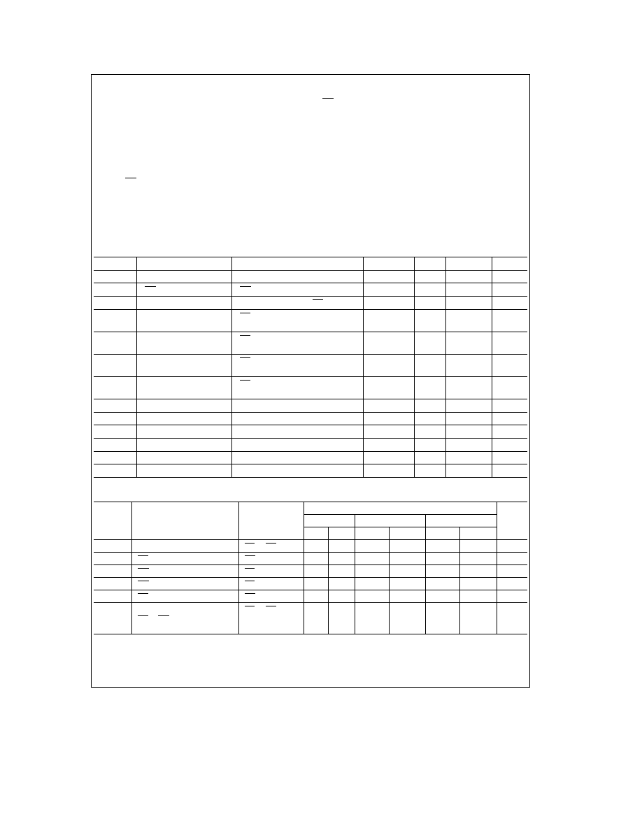
DC Electrical Characteristics
Symbol
Parameter
Conditions
Min
Typ
Max
Units
I
LI
Input Load Current
V
IN
e
V
CC
or GND
0 01
1
m
A
I
PP
OE V
PP
Load Current
OE V
PP
e
V
CC
or GND
10
m
A
I
LO
Output Leakage Current
V
OUT
e
V
CC
or GND CE
e
V
IH
0 01
1
m
A
I
CC1
V
CC
Current (Active)
CE
e
V
IL
f
e
5 MHz
5
20
mA
TTL Inputs
Inputs
e
V
IH
or V
IL
I O
e
0 mA
I
CC2
V
CC
Current (Active)
CE
e
GND f
e
5 MHz
3
10
mA
CMOS Inputs
Inputs
e
V
CC
or GND I O
e
0 mA
I
CCSB1
V
CC
Current (Standby)
CE
e
V
IH
0 1
1
mA
TTL Inputs
I
CCSB2
V
CC
Current (Standby)
CE
e
V
CC
0 5
100
m
A
CMOS Inputs
V
IL
Input Low Voltage
b
0 2
0 8
V
V
IH
Input High Voltage
2 0
V
CC
a
1
V
V
OL1
Output Low Voltage
I
OL
e
2 1 mA
0 45
V
V
OH1
Output High Voltage
I
OH
e b
400 mA
2 4
V
V
OL2
Output Low Voltage
I
OL
e
10 mA
0 1
V
V
OH2
Output High Voltage
I
OH
e b
10 mA
V
CC
b
0 1
V
AC Electrical Characteristics
NMC27C32B
Symbol
Parameter
Conditions
Q150
Q200 QE200
Q250
Units
Min
Max
Min
Max
Min
Max
t
ACC
Address to Output Delay
CE
e
OE
e
V
IL
150
200
250
ns
t
CE
CE to Output Delay
OE
e
V
IL
150
200
250
ns
t
OE
OE to Output Delay
CE
e
V
IL
60
60
70
ns
t
DF
OE High to Output Float
CE
e
V
IL
0
50
0
60
0
70
ns
t
CF
CE High to Output Float
OE
e
V
IL
0
50
0
60
0
60
ns
t
OH
Output Hold from Addresses
CE
e
OE
e
V
IL
CE or OE Whichever
0
0
0
ns
Occurred First
http
www national com
3
Capacitance
T
A
e a
25 C f
e
1 MHz (Note 2)
Symbol
Parameter
Conditions
Typ
Max
Units
C
IN1
Input Capacitance except OE V
PP
V
IN
e
0V
6
12
pF
C
IN2
OE V
PP
Input Capacitance
V
IN
e
0V
16
20
pF
C
OUT
Output Capacitance
V
OUT
e
0V
9
12
pF
AC Test Conditions
Output Load
1 TTL Gate and
C
L
e
100 pF (Note 8)
Input Rise and Fall Times
s
5 ns
Input Pulse Levels
0 45V to 2 4V
Timing Measurement Reference Level
Inputs
0 8V and 2V
Outputs
0 8V and 2V
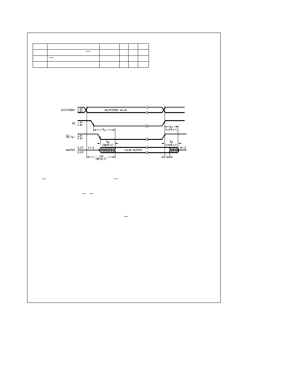
AC Waveforms
(Note 7)
TL D 8827 � 3
Note 1
Stresses above those listed under ``Absolute Maximum Ratings'' may cause permanent damage to the device This is a stress rating only and functional
operation of the device at these or any other conditions above those indicated in the operational sections of this specification is not implied Exposure to absolute
maximum rating conditions for extended periods may affect device reliability
Note 2
This parameter is only sampled and is not 100% tested
Note 3
OE may be delayed up to t
ACC
b
t
OE
after the falling edge of CE without impacting t
ACC
Note 4
The t
DF
and t
CF
compare level is determined as follows
High to TRI-STATE the measured V
OH1
(DC)
b
0 10V
Low to TRI-STATE the measured V
OL1
(DC)
a
0 10V
Note 5
TRI-STATE may be attained using OE or CE
Note 6
The power switching characteristics of EPROMs require careful device decoupling It is recommended that at least a 0 1 mF ceramic capacitor be used on
every device between V
CC
and GND
Note 7
The outputs must be restricted to V
CC
a
1 0V to avoid latch-up and device damage
Note 8
1 TTL Gate I
OL
e
1 6 mA I
OH
e b
400 mA
C
L
100 pF includes fixture capacitance
Note 9
Inputs and outputs can undershoot to
b
2 0V for 20 ns Max except for OE V
PP
which cannot exceed
b
0 2V
Note 10
Typical values are for T
A
e
25 C and nominal supply voltages
http
www national com
4
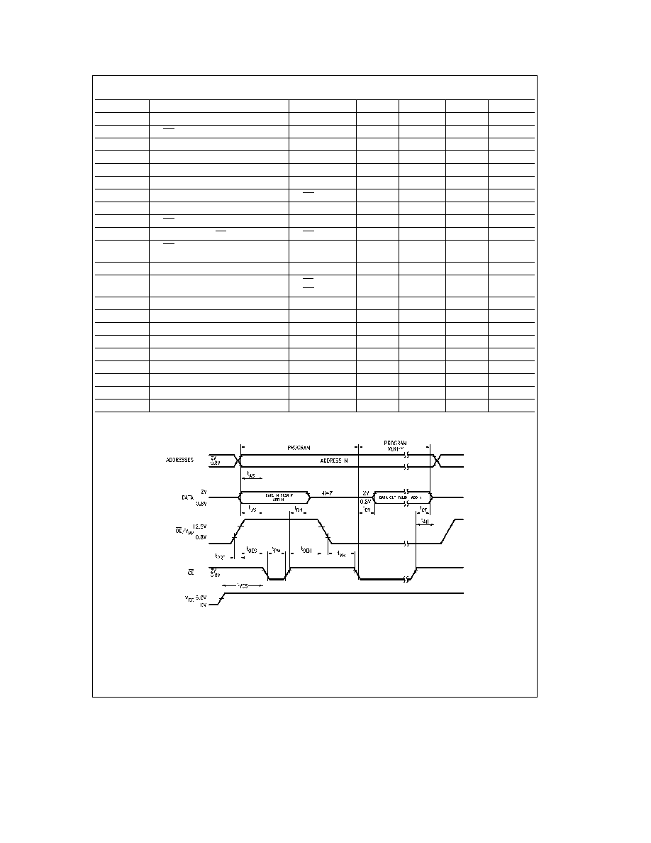
Programming Characteristics
(Notes 1 2 3
4)
Symbol
Parameter
Conditions
Min
Typ
Max
Units
t
AS
Address Setup Time
1
m
s
t
OES
OE Setup Time
1
m
s
t
DS
Data Setup Time
1
m
s
t
VCS
V
CC
Setup Time
1
m
s
t
AH
Address Hold Time
0
m
s
t
DH
Data Hold Time
1
m
s
t
CF
Chip Enable to Output Float Delay
OE
e
V
IL
0
60
ns
t
PW
Program Pulse Width
95
100
105
m
s
t
OEH
OE Hold Time
1
m
s
t
DV
Data Valid from CE
OE
e
V
IL
250
ns
t
PRT
OE Pulse Rise Time
50
ns
During Programming
t
VR
V
PP
Recovery Time
1
m
s
I
PP
V
PP
Supply Current During
CE
e
V
IL
30
mA
Programming Pulse
OE
e
V
PP
I
CC
V
CC
Supply Current
10
mA
T
A
Temperature Ambient
20
25
30
C
V
CC
Power Supply Voltage
6 0
6 25
6 5
V
V
PP
Programming Supply Voltage
12 5
12 75
13 0
V
t
FR
Input Rise Fall Time
5
ns
V
IL
Input Low Voltage
0 0
0 45
V
V
IH
Input High Voltage
2 4
4 0
V
t
IN
Input Timing Reference Voltage
0 8
2 0
V
t
OUT
Output Timing Reference Voltage
0 8
2 0
V
Programming Waveforms
TL D 8827 � 4
Note 1
National's standard product warranty applies only to devices programmed to specifications described herein
Note 2
V
CC
must be applied simultaneously or before V
PP
and removed simultaneously or after V
PP
The EPROM must not be inserted into or removed from a
board with voltage applied to V
PP
or V
CC
Note 3
The maximum absolute allowable voltage which may be applied to the V
PP
pin during programming is 14V Care must be taken when switching the V
PP
supply to prevent any overshoot from exceeding this 14V maximum specification At least a 0 1 mF capacitor is required across V
CC
to GND to suppress spurious
voltage transients which may damage the device
Note 4
Programming and program verify are tested with the fast Program Algorithm at typical power supply voltages and timings
http
www national com
5

Fast Programming Algorithm Flow Chart
(Note 4)
TL D 8827 � 5
FIGURE 1
http
www national com
6
Functional Description
DEVICE OPERATION
The six modes of operation of the NMC27C32B are listed in
Table I A single 5V power supply is required in the read
mode All inputs are TTL levels except for OE V
PP
during
programming In the program mode the OE V
PP
input is
pulsed from a TTL low level to 12 75V
Read Mode
The NMC27C32B has two control functions both of which
must be logically active in order to obtain data at the out-
puts Chip Enable (CE) is the power control and should be
used for device selection Output Enable (OE) is the output
control and should be used to gate data to the output pins
independent of device selection Assuming that addresses
are stable address access time (t
ACC
) is equal to the delay
from CE to output (t
CE
) Data is available at the outputs t
OE
after the falling edge of OE assuming that CE has been low
and addresses have been stable for at least t
ACC
� t
OE
The sense amps are clocked for fast access time V
CC
should therefore be maintained at operating voltage during
read and verify If V
CC
temporarily drops below the spec
voltage (but not to ground) an address transition must be
performed after the drop to ensure proper output data
Standby Mode
The NMC27C32B has a standby mode which reduces the
active power dissipation by 99% from 55 mW to 0 55 mW
The NMC27C32B is placed in the standby mode by applying
a CMOS high signal to the CE input When in standby mode
the outputs are in a high impedance state independent of
the OE input
Output OR-Tying
Because EPROMs are usually used in larger memory ar-
rays National has provided a 2-line control function that
accommodates this use of multiple memory connection
The 2-line control function allows for
a The lowest possible memory power dissipation and
b complete assurance that output bus contention will not
occur
To most efficiently use these two control lines it is recom-
mended that CE (pin 18) be decoded and used as the pri-
mary device selecting function while OE (pin 20) be made a
common connection to all devices in the array and connect-
ed to the READ line from the system control bus This as-
sures that all deselected memory devices are in their low
power standby modes and that the output pins are active
only when data is desired from a particular memory device
Programming
CAUTION Exceeding 14V on pin 20 OE V
PP
will damage
the NMC27C32B
Initially and after each erasure all bits of the NMC27C32B
are in the ``1'' state Data is introduced by selectively pro-
gramming ``0s'' into the desired bit locations Although only
``0s'' will be programmed both ``1s'' and ``0s'' can be pre-
sented in the data word The only way to change a ``0'' to a
``1'' is by ultraviolet light erasure
The NMC27C32B is in the programming mode when
OE V
PP
is at 12 75V It is required that at least a 0 1 mF
capacitor be placed across V
CC
and ground to suppress
spurious voltage transients which may damage the device
The data to be programmed is applied 8 bits in parallel to
the data output pins The levels required for the address
and data inputs are TTL
When the address and data are stable an active low TTL
program pulse is applied to the CE input A program pulse
must be applied at each address location to be pro-
grammed The NMC27C32B is programmed with the Fast
Programming Algorithm shown in
Figure 1 Each Address is
programmed with a series of 100 ms pulses until it verifies
good up to a maximum of 25 pulses Most memory cells will
Program with a single 100 ms pulse
Note
Some programmer manufactures due to equipment limitation may of-
fer interactive program Algorithm (Shown in
Figure 2 )
The NMC27C32B must not be programmed with a DC signal
applied to the CE input
Programming multiple NMC27C32Bs in parallel with the
same data can be easily accomplished due to the simplicity
of the programming requirements Like inputs of the paral-
leled NMC27C32B may be connected together when they
are programmed with the same data A low level TTL pulse
applied
to
the
CE
input
programs
the
paralleled
NMC27C32B
TABLE I Mode Selection
Pins
CE
OE V
PP
V
CC
Outputs
Mode
(18)
(20)
(24)
(9 � 11 13 � 17)
Read
V
IL
V
IL
5V
D
OUT
Standby
V
IH
Don't Care
5V
Hi-Z
Program
V
IL
12 75V
6 25V
D
IN
Program Verify
V
IL
V
IL
6 25V
D
OUT
Program Inhibit
V
IH
12 75V
6 25V
Hi-Z
Output Disable
Don't Care
V
IH
5V
Hi-Z
http
www national com
7
Functional Description
(Continued)
Program Inhibit
Programming multiple NMC27C32B in parallel with different
data is also easily accomplished Except for CE all like in-
puts (including OE) of the parallel NMC27C32B may be
common A TTL low level program pulse applied to an
NMC27C32B's CE input with OE V
PP
at 12 75V will pro-
gram that NMC27C32B A TTL high level CE input inhibits
the other NMC27C32B from being programmed
Program Verify
A verify should be performed on the programmed bit to de-
termine whether they were correctly programmed The veri-
fy is accomplished with OE V
PP
and CE at V
IL
Data should
be verified t
DV
after the falling edge of CE
MANUFACTURER'S IDENTIFICATION CODE
The NMC27C32B has a manufacturer's identification code
to aid in programming The code shown in Table II is two
bytes wide and is stored in a ROM configuration on the chip
It identifies the manufacturer and the device type The code
for the NMC27C32B is ``8F01'' where ``8F'' designates that
it is made by National Semiconductor and ``01'' designates
a 32k part
The code is accessed by applying 12 0V
g
0 5V to address
pin A9 Addresses A1 � A8 A10 � A11 CE and OE are held
at V
IL
Address A0 is held at V
IL
for the manufacturer's
code and at V
IH
for the device code The code is read out
on the 8 data pins Proper code access is only guaranteed
at 25 C
g
5 C
The primary purpose of the manufacturer's identification
code is automatic programming control When the device is
inserted in an EPROM programmer socket the programmer
reads the code and then automatically calls up the specific
programming algorithm for the part This automatic pro-
gramming control is only possible with programmers which
have the capability of reading the code
ERASURE CHARACTERISTICS
The erasure characteristics of the NMC27C32B are such
that erasure begins to occur when exposed to light with
wavelengths shorter than approximately 4000 Angstroms
( ) It should be noted that sunlight and certain types of
fluorescent lamps have wavelengths in the 3000 � 4000
range After programming opaque labels should be placed
over the NMC27C32B's window to prevent unintentional
erasure Covering the window will also prevent temporary
functional failure due to the generation of photo currents
The recommended erasure procedure for the NMC27C32B
is exposure to short wave ultraviolet light which has a wave-
length of 2537
The integrated dose (i e UV intensity
c
exposure time) for erasure should be a minimum of
15 W-sec cm
2
The NMC27C32B should be placed within 1 inch of the
lamp tubes during erasure Some lamps have a filter on their
tubes which should be removed before erasure Table III
shows the minimum NMC27C32B erasure time for various
light intensities
An erasure system should be calibrated periodically The
distance from lamp to unit should be maintained at one inch
The erasure time increases as the square of the distance (If
distance is doubled the erasure time increases by a factor of
4 ) Lamps lose intensity as they age When a lamp is
changed the distance has changed or the lamp has aged
the system should be checked to make certain full erasure
is occurring Incomplete erasure will cause symptoms that
can be misleading Programmers components and even
system designs have been erroneously suspected when in-
complete erasure was the problem
SYSTEM CONSIDERATION
The power switching characteristics of EPROMs require
careful decoupling of the devices The supply current I
CC
has three segments that are of interest to the system de-
signer
the standby current level the active current level
and the transient current peaks that are produced by volt-
age transitions on input pins The magnitude of these tran-
sient current peaks is dependent on the output capacitance
loading of the device The associated V
CC
transient voltage
peaks can be suppressed by properly selected decoupling
capacitors It is recommended that at least a 0 1 mF ceramic
capacitor be used on every device between V
CC
and GND
This should be a high frequency capacitor of low inherent
inductance In addition at least a 4 7 mF bulk electrolytic
capacitor should be used between V
CC
and GND for each
eight devices The bulk capacitor should be located near
where the power supply is connected to the array The pur-
pose of the bulk capacitor is to overcome the voltage drop
caused by the inductive effects of the PC board traces
TABLE II Manufacturer's Identification Code
Pins
A0
O
7
O
6
O
5
O
4
O
3
O
2
O
1
O
0
Hex
(8)
(17)
(16)
(15)
(14)
(13)
(11)
(10)
(9)
Data
Manufacturer Code
V
IL
1
0
0
0
1
1
1
1
8F
Device Code
V
IH
0
0
0
0
0
0
0
1
01
TABLE III Minimum NMC27C32B Erasure Time
Light Intensity
Erasure Time
(mW cm
2
)
(Minutes)
15 000
20
10 000
25
5 000
50
http
www national com
8

http
www national com
9
NMC27C32B
32768-Bit
(4096
x
8
)
CMOS
EPROM
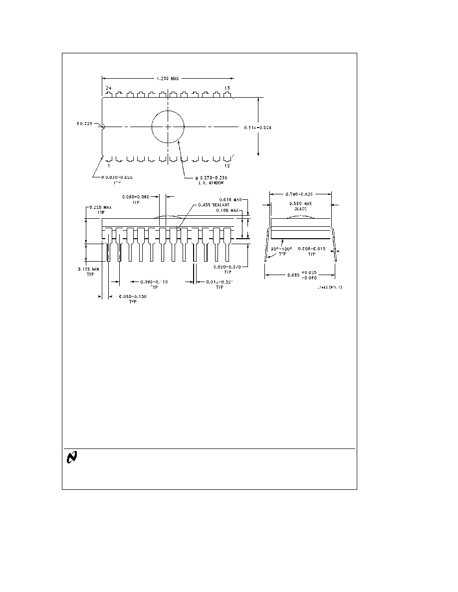
Physical Dimensions
inches (millimeters) unless otherwise noted
UV Window Cavity Dual-In-Line Cerdip Package (JQ)
Order Number NMC27C32BQ
NS Package Number J24AQ
LIFE SUPPORT POLICY
NATIONAL'S PRODUCTS ARE NOT AUTHORIZED FOR USE AS CRITICAL COMPONENTS IN LIFE SUPPORT
DEVICES OR SYSTEMS WITHOUT THE EXPRESS WRITTEN APPROVAL OF THE PRESIDENT OF NATIONAL
SEMICONDUCTOR CORPORATION As used herein
1 Life support devices or systems are devices or
2 A critical component is any component of a life
systems which (a) are intended for surgical implant
support device or system whose failure to perform can
into the body or (b) support or sustain life and whose
be reasonably expected to cause the failure of the life
failure to perform when properly used in accordance
support device or system or to affect its safety or
with instructions for use provided in the labeling can
effectiveness
be reasonably expected to result in a significant injury
to the user
National Semiconductor
National Semiconductor
National Semiconductor
National Semiconductor
Corporation
Europe
Southeast Asia
Japan Ltd
Fax a49 (0) 180-530 85 86
Fax (852) 2376 3901
Tel 81-3-5620-7561
Americas
Email europe support nsc com
Email sea support nsc com
Fax 81-3-5620-6179
Tel 1(800) 272-9959
Deutsch Tel a49 (0) 180-530 85 85
Fax 1(800) 737-7018
English
Tel a49 (0) 180-532 78 32
Email support nsc com
Fran ais Tel a49 (0) 180-532 93 58
Italiano
Tel a49 (0) 180-534 16 80
http
www national com
National does not assume any responsibility for use of any circuitry described no circuit patent licenses are implied and National reserves the right at any time without notice to change said circuitry and specifications