 | –≠–ª–µ–∫—Ç—Ä–æ–Ω–Ω—ã–π –∫–æ–º–ø–æ–Ω–µ–Ω—Ç: NS32829 | –°–∫–∞—á–∞—Ç—å:  PDF PDF  ZIP ZIP |
TL F 8649
DP8428NS32828
DP8429NS32829
1
Megabit
High
Speed
Dynamic
RAM
ControllerDrivers
September 1991
DP8428 NS32828 DP8429 NS32829
1 Megabit High Speed Dynamic RAM Controller Drivers
General Description
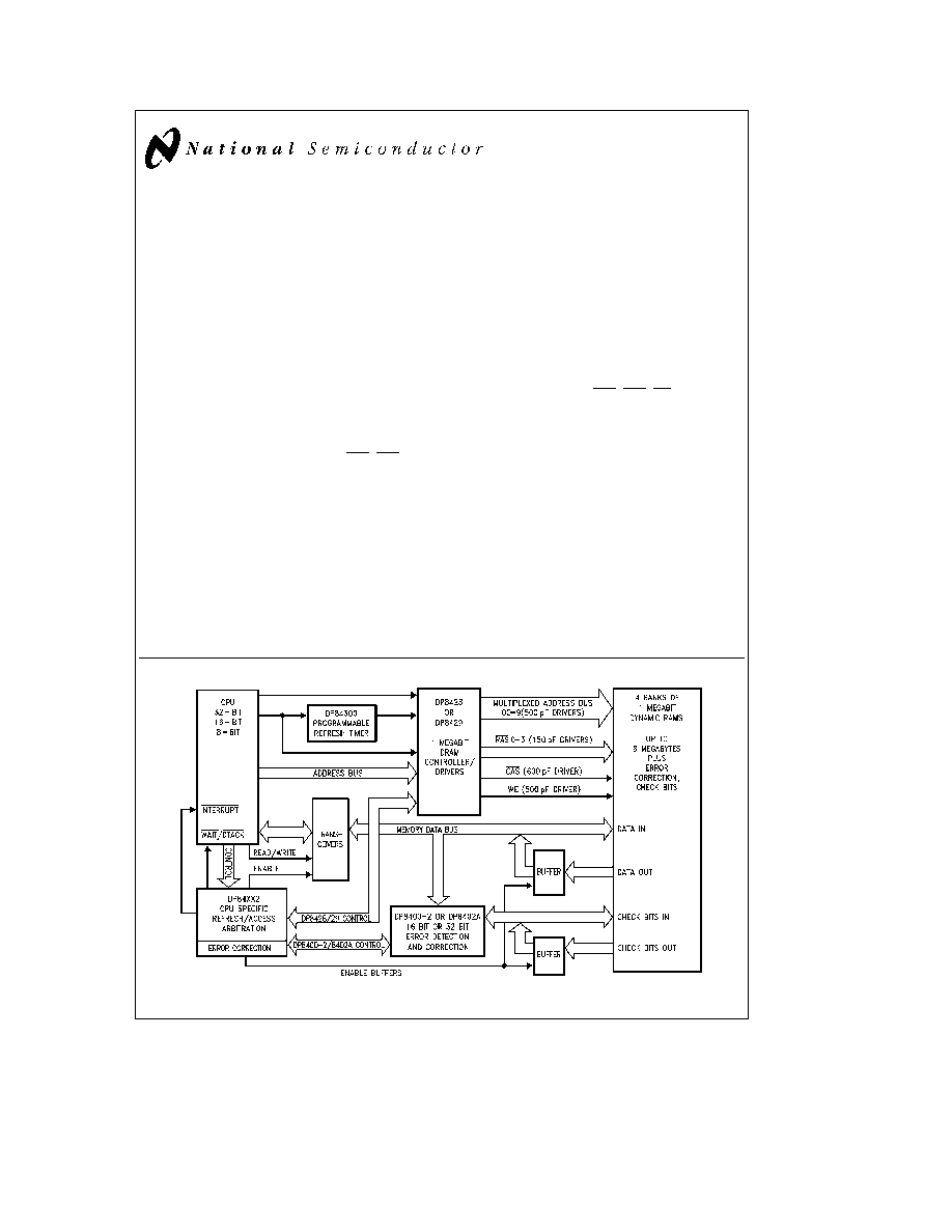
The DP8428 and DP8429 1M DRAM Controller Drivers are
designed to provide ``No-Waitstate'' CPU interface to Dy-
namic RAM arrays of up to 8 Mbytes and larger The
DP8428 and DP8429 are tailored for 32-bit and 16-bit sys-
tem requirements respectively Both devices are fabricated
using National's new oxide isolated Advanced Low power
Schottky (ALS) process and use design techniques which
enable them to significantly out-perform all other LSI or dis-
crete alternatives in speed level of integration and power
consumption
Each device integrates the following critical 1M DRAM con-
troller functions on a single monolithic device ultra precise
delay line 9 bit refresh counter fall-through row column
and bank select input latches Row Column address mux-
ing logic on-board high capacitive-load RAS CAS Write
Enable and Address output drivers and precise control sig-
nal timing for all the above
In order to specify each device for ``true'' worst case operat-
ing conditions all timing parameters are guaranteed while
the chip is driving the capacitive load of 88 DRAMs includ-
ing trace capacitance The chip's delay timing logic makes
use of a patented new delay line technique which keeps AC
skew to
g
3 ns over the full V
CC
range of
g
10% and tem-
perature range of
b
55 C to
a
125 C The DP8428 and
DP8429 guarantee a maximum RASIN to CASOUT delay of
80 ns or 70 ns even while driving an 8 Mbyte memory array
with error correction check bits included Two speed select-
ed options of these devices are shown in the switching
characteristics section of this document
(Continued)
Features
Y
Makes DRAM interface and refresh tasks appear virtu-
ally transparent to the CPU making DRAMs as easy to
use as static RAMs
Y
Specifically designed to eliminate CPU wait states up to
10 MHz or beyond
Y
Eliminates 20 discrete components for significant board
real estate reduction system power savings and the
elimination of chip-to-chip AC skewing
Y
On-board ultra precise delay line
Y
On-board high capacitive RAS CAS WE and Address
drivers (specified driving 88 DRAMs directly)
Y
AC specified for directly addressing up to 8 Mbytes
Y
Low power high speed bipolar oxide isolated process
Y
Downward pin and function compatible with 256k
DRAM Controller Drivers DP8409A DP8417 DP8418
and DP8419
Contents
Y
System and Device Block Diagrams
Y
Recommended Companion Components
Y
Device Connection Diagrams and Pin Definitions
Y
Device Differences
DP8428 vs DP8429
Y
Mode of Operation
(Descriptions and Timing Diagrams)
Y
Application Description and Diagrams
Y
DC AC Electrical Specifications Timing Diagrams and
Test Conditions
System Diagram
TL F 8649 ≠ 1
TRI-STATE
is a registered trademark of National Semiconductor Corp
PAL
is a registered trademark of and used under license with Monolithic Memories Inc
C1995 National Semiconductor Corporation
RRD-B30M105 Printed in U S A
General Description
(Continued)
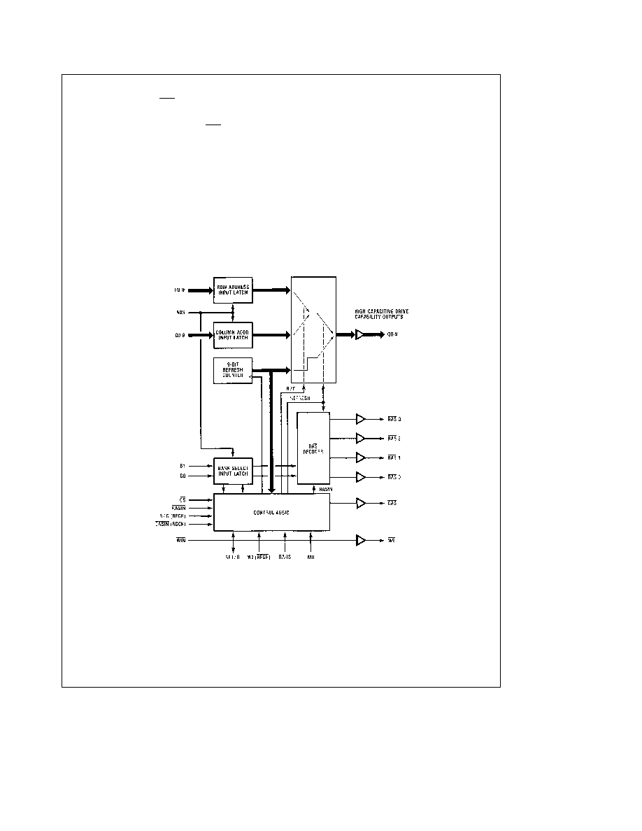
With its four independent RAS outputs and ten multiplexed
address outputs the DP8429 can support up to four banks
of 64k 256k or 1M DRAMs Two bank select pins B1 and
B0 are decoded to activate one of the RAS signals during
an access leaving the three non-selected banks in the
standby mode (less than one tenth of the operating power)
with data outputs in TRI-STATE
The DP8428's one Bank
Select pin B1 enables 2 banks automatically during an ac-
cess in order to provide an optimum interface for 32-bit mi-
croprocessors
The DP8428 and DP8429 each have two mode-select pins
allowing for two refresh modes and two access modes Re-
fresh and access timing may be controlled either externally
or automatically The automatic modes require a minimum
of input control signals
A refresh counter is on-chip and is multiplexed with the row
and column inputs Its contents appear at the address out-
puts of the DP8428 or DP8429 during any refresh and are
incremented at the completion of the refresh Row Column
and bank address latches are also on-chip However if the
address inputs to the DP8428 or DP8429 are valid through-
out the duration of the access these latches may be operat-
ed in the fall-through mode
Each device is available in either the 52 pin Ceramic DIP or
the low cost JEDEC standard 68 pin Plastic Chip Carrier
(PCC) package
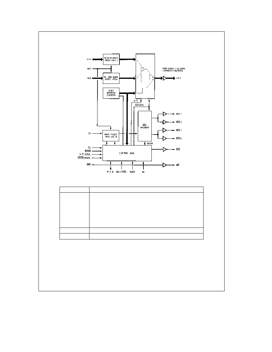
Functional Block Diagrams
DP8429
TL F 8649 ≠ 2
2
Functional Block Diagrams
(Continued)
DP8428
TL F 8649 ≠ 3
System Companion Components
Device
Function
DP84300
Programmable Refresh Timer for DP84xx DRAM Controller
DP84412
NS32008 16 32 to DP8409A 17 18 19 28 29 Interface
DP84512
NS32332 to DP8417 18 19 28 29 Interface
DP84322
68000 08 10 to DP8409A 17 18 19 28 29 Interface (up to 8 MHz)
DP84422
68000 08 10 to DP8409A 17 18 19 28 29 Interface (up to 12 5 MHz)
DP84522
68020 to DP8417 18 19 28 29 Interface
DP84432
8086 88 186 188 to DP8409A 17 18 19 28 29 Interface
DP84532
80286 to DP8409A 17 18 19 28 29 Interface
DP8400-2
16-Bit Expandable Error Checker Corrector (E2C2)
DP8402A
32-Bit Error Detector And Corrector (EDAC)
3
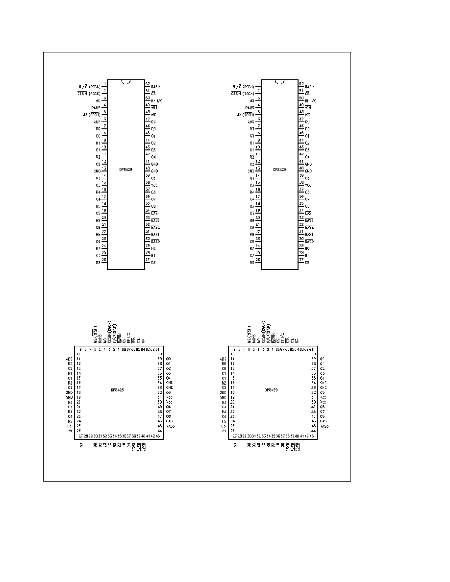
Connection Diagrams
Dual-In-Line Package
TL F 8649 ≠ 4
Dual-In-Line Package
TL F 8649 ≠ 5
Order Number DP8428D-70 DP8428D-80 or
DP8429D-70 DP8429D-80
See NS Package Number D52A
Plastic Chip Carrier Package
TL F 8649 ≠ 6
Plastic Chip Carrier Package
TL F 8649 ≠ 7
Order Number DP8428V-70 DP8428V-80 or
DP8429V-70 DP8429V-80
See NS Package Number V68A
4
DP8428 vs DP8429
The DP8428 DYNAMIC RAM CONTROLLER DRIVER is
identical to the DP8429 with the exception of two functional
differences incorporated to improve performance with 32-bit
microprocessors
1) Pin 28 (B1) is used to enable disable a pair of RAS out-
puts and pin 29 (B0 on the DP8429) is a no connect
When B1 is low RAS0 and RAS1 are enabled such that
they both go low during an access When B1 is high
RAS2 and RAS3 are enabled This feature is useful when
driving words of 32 bits or more since each RAS would
be driving only one half of the word By distributing the
load on each RAS line in this way the DP8428 will meet
the same AC specifications driving 2 banks of 32 DRAMs
each as the DP8429 does driving 4 banks of 16 bits each
2) The hidden refresh function available on the DP8429 has
been disabled on the DP8428 in order to reduce the
amount of setup time necessary from CS going low to
RASIN going low during an access of DRAM This param-
eter called t
CSRL1
is 5 ns for the DP8428 whereas it is
34 ns for the DP8429 The hidden refresh function al-
lowed only a very small increase in system performance
at microprocessor frequencies of 10 MHz and above
Pin Definitions
V
CC
GND GND
b
V
CC
e
5V
g
10%
The three supply
pins have been assigned to the center of the package to
reduce voltage drops both DC and AC There are two
ground pins to reduce the low level noise The second
ground pin is located two pins from V
CC
so that decoupling
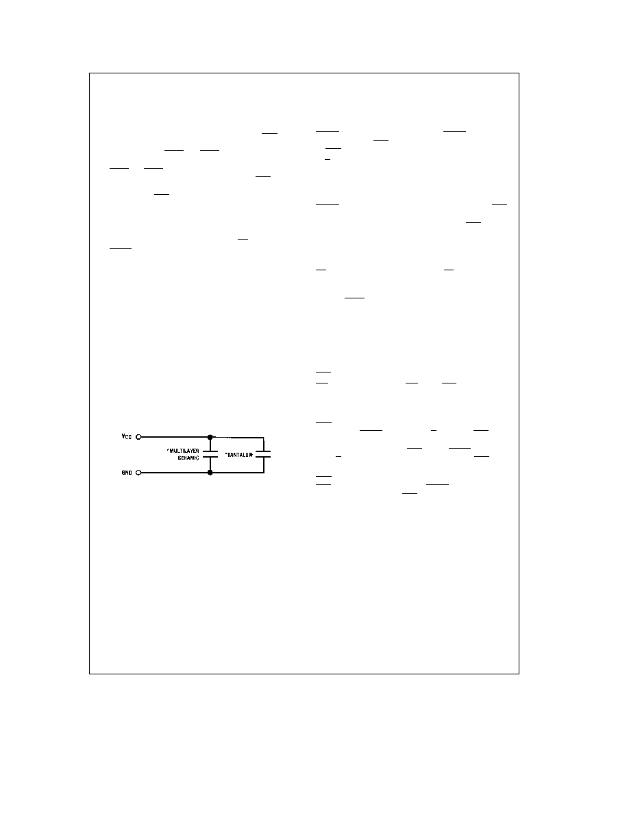
capacitors can be inserted directly next to these pins It is
important to adequately decouple this device due to the
high switching currents that will occur when all 10 address
bits change in the same direction simultaneously A recom-
mended solution would be a 1 mF multilayer ceramic capaci-
tor in parallel with a low-voltage tantalum capacitor both
connected as close as possible to GND and V
CC
to reduce
lead inductance See Figure below
TL F 8649 ≠ 8
Capacitor values should be chosen depending on the particular application
R0 ≠ R9 Row Address Inputs
C0 ≠ C9 Column Address Inputs
Q0 ≠ Q9 Multiplexed Address Outputs ≠
This address is
selected from the Row Address Input Latch the Column
Address Input Latch or the Refresh Counter
RASIN Row Address Strobe Input ≠
RASIN directly con-
trols the selected RAS output when in an access mode and
all RAS outputs during hidden or external refresh
R C (RFCK) ≠
In the auto-modes this pin is the external
refresh clock input one refresh cycle should be performed
each clock period In the external access mode it is Row
Column Select Input which enables either the row or column
address input latch onto the output bus
CASIN (RGCK) ≠
In the auto-modes this pin is the RAS
Generator Clock input In external access mode it is the
Column Address Strobe input which controls CAS directly
once columns are enabled on the address outputs
ADS Address (Latch) Strobe Input ≠
Row Address Col-
umn Address and Bank Select Latches are fall-through with
ADS high latching occurs on high-to-low transition of ADS
CS Chip Select Input ≠
When high CS disables all ac-
cesses Refreshing however in both modes 0 and 1 is not
affected by this pin
M0 M2 (RFSH) Mode Control Inputs ≠
These pins select
one of the four available operational modes of the DP8429
(see Table III)
RFI 0 Refresh Input Output ≠
In the auto-modes this pin
is the Refresh Request Output It goes low following RFCK
indicating that no hidden refresh was performed while RFCK
was high When this pin is set low by an external gate the
on-chip refresh counter is reset to all zeroes
WIN Write Enable Input
WE Write Enable Output ≠
WE follows WIN unconditionally
RAHS Row Address Hold Time Select ≠
Selects the
t
RAH
to be guaranteed by the DP8428 or DP8429 delay line
to allow for the use of fast or slow DRAMs
CAS Column Address Strobe Output ≠
In mode 5 and in
mode 4 with CASIN low before R C goes low CAS goes
low automatically after the column address is valid on the
address outputs In mode 4 CAS follows CASIN directly af-
ter R C goes low allowing for nibble accessing CAS is al-
ways high during refresh
RAS 0 ≠ 3 Row Address Strobe Outputs ≠
The enabled
RAS output (see Table II) follows RASIN directly during an
access During refresh all RAS outputs are enabled
5