
TL EE 8525
NS32C016-10NS32C016-15
High-Performance
Microprocessors
PRELIMINARY
July 1989
NS32C016-10 NS32C016-15
High-Performance Microprocessors
General Description
The NS32C016 is a 32-bit CMOS microprocessor with TTL
compatible inputs The NS32C016 has a 16M byte linear
address space and a 16-bit external data bus It is fabricat-
ed with National Semiconductor's advanced CMOS process
and is fully object code compatible with other Series
32000
CPU's The NS32C016 has a 32-bit ALU eight 32-
bit general purpose registers an eight-byte prefetch queue
and a highly symmetric architecture It also incorporates a
slave processor interface and provides for full virtual memo-
ry capability in conjunction with the NS32082 memory man-
agement unit (MMU) High performance floating-point in-
structions are provided with the NS32081 floating-point unit
(FPU) The NS32C016 is intended for a wide range of high
performance computer applications
Features
Y
32-bit architecture and implementation
Y
16M byte uniform addressing space
Y
Powerful instruction set
General 2-address capability
Very high degree of symmetry
Addressing modes optimized for high-level
Language references
Y
High-speed CMOS technology
Y
TTL compatible inputs
Y
Single 5V supply
Y
48-pin dual-in-line package
Block Diagram
TL EE 8525 � 1
STARPLEX II
TM
is a trademark of National Semiconductor Corp
Series 32000
and TRI-STATE
are registered trademarks of National Semiconductor Corp
C1995 National Semiconductor Corporation
RRD-B30M105 Printed in U S A

Table of Contents
1 0 PRODUCT INTRODUCTION
2 0 ARCHITECTURAL DESCRIPTION
2 1 Programming Model
2 1 1 General Purpose Registers
2 1 2 Dedicated Registers
2 1 3 The Configuration Register (CFG)
2 1 4 Memory Organization
2 1 5 Dedicated Tables
2 2 Instruction Set
2 2 1 General Instruction Format
2 2 2 Addressing Modes
2 2 3 Instruction Set Summary
3 0 FUNCTIONAL DESCRIPTION
3 1 Power and Grounding
3 2 Clocking
3 3 Resetting
3 4 Bus Cycles
3 4 1 Cycle Extension
3 4 2 Bus Status
3 4 3 Data Access Sequences
3 4 3 1 Bit Accesses
3 4 3 2 Bit Field Accesses
3 4 3 3 Extending Multiply Accesses
3 4 4 Instruction Fetches
3 4 5 Interrupt Control Cycles
3 4 6 Slave Processor Communication
3 4 6 1 Slave Processor Bus Cycles
3 4 6 2 Slave Operand Transfer Sequences
3 5 Memory Management Option
3 5 1 Address Translation Strap
3 5 2 Translated Bus Timing
3 5 3 The FLT (Float) Pin
3 5 4 Aborting Bus Cycles
3 5 4 1 The Abort Interrupt
3 5 4 2 Hardware Considerations
3 6 Bus Access Control
3 7 Instruction Status
3 0 FUNCTIONAL DESCRIPTION
(Continued)
3 8 NS32C016 Interrupt Structure
3 8 1 General Interrupt Trap Sequence
3 8 2 Interrupt Trap Return
3 8 3 Maskable Interrupts (The INT Pin)
3 8 3 1 Non-Vectored Mode
3 8 3 2 Vectored Mode Non-Cascaded Case
3 8 3 3 Vectored Mode Cascaded Case
3 8 4 Non-Maskable Interrupt (The NMI Pin)
3 8 5 Traps
3 8 6 Prioritization
3 8 7 Interrupt Trap Sequences Detail Flow
3 8 7 1 Maskable Non-Maskable Interrupt Se-
quence
3 8 7 2 Trap Sequence Traps Other Than Trace
3 8 7 3 Trace Trap Sequence
3 8 7 4 Abort Sequence
3 9 Slave Processor Instructions
3 9 1 Slave Processor Protocol
3 9 2 Floating Point Instructions
3 9 3 Memory Management Instructions
3 9 4 Custom Slave Instructions
4 0 DEVICE SPECIFICATIONS
4 1 NS32C016 Pin Descriptions
4 1 1 Supplies
4 1 2 Input Signals
4 1 3 Output Signals
4 1 4 Input-Output Signals
4 2 Absolute Maximum Ratings
4 3 Electrical Characteristics
4 4 Switching Characteristics
4 4 1 Definitions
4 4 2 Timing Tables
4 4 2 1 Output Signals Internal Propagation De-
lays
4 4 2 2 Input Signal Requirements
4 4 2 3 Clocking Requirements
APPENDIX A INSTRUCTION FORMATS
APPENDIX B INTERFACING SUGGESTIONS
List of Illustrations
The General and Dedicated Registers
2-1
Processor Status Register
2-2
CFG Register
2-3
Module Descriptor Format
2-4
A Sample Link Table
2-5
General Instruction Format
2-6
Index Byte Format
2-7
Displacement Encodings
2-8
Recommended Supply Connections
3-1
Clock Timing Relationships
3-2
2

List of Illustrations
(Continued)
Power-On Reset Requirements
3-3
General Reset Timing
3-4
Recommended Reset Connections Non-Memory-Managed System
3-5a
Recommended Reset Connections Memory-Managed System
3-5b
Bus Connections
3-6
Read Cycle Timing
3-7
Write Cycle Timing
3-8
RDY Pin Timing
3-9
Extended Cycle Example
3-10
Memory Interface
3-11
Slave Processor Connections
3-12
CPU Read from Slave Processor
3-13
CPU Write to Slave Processor
3-14
Read Cycle with Address Translation (CPU Action)
3-15
Write Cycle with Address Translation (CPU Action)
3-16
Memory-Managed Read Cycle
3-17
Memory-Managed Write Cycle
3-18
FLT Timing
3-19
HOLD Timing Bus Initially Idle
3-20
HOLD Timing Bus Initially Not Idle
3-21
Interrupt Dispatch and Cascade Tables
3-22
Interrupt Trap Service Routine Calling Sequence
3-23
Return from Trap (RETT n) Instruction Flow
3-24
Return from Interrupt (RET I) Instruction Flow
3-25
Interrupt Control Unit Connections (16 Levels)
3-26
Cascaded Interrupt Control Unit Connections
3-27
Slave Processor Status Word Format
3-30
Connection Diagram
4-1
Timing Specification Standard (CMOS Output Signals)
4-2
Timing Specification Standard (TTL Input Signals)
4-3
Write Cycle
4-4
Read Cycle
4-5
Floating by HOLD Timing (CPU Not Idle Initially)
4-6
Floating by HOLD Timing (CPU Initially Idle)
4-7
Release from HOLD
4-8
FLT Initiated Cycle Timing
4-9
Release from FLT Timing
4-10
Ready Sampling (CPU Initially READY)
4-11
Ready Sampling (CPU Initially NOT READY)
4-12
Slave Processor Write Timing
4-13
Slave Processor Read Timing
4-14
SPC Non-Forcing Delay
4-15
Reset Configuration Timing
4-16
Clock Waveforms
4-17
Relationship of PFS to Clock Cycles
4-18
Guaranteed Delay PFS to Non-Sequential Fetch
4-19a
Guaranteed Delay Non-Sequential Fetch to PFS
4-19b
Relationship of ILO to First Operand Cycle of an Interlocked Instruction
4-20a
Relationship of ILO to Last Operand Cycle of an Interlocked Instruction
4-20b
Relationship of ILO to Any Clock Cycle
4-21
U S Relationship to any Bus Cycle � Guaranteed Valid Interval
4-22
Abort Timing FLT Not Applied
4-23
Abort Timing FLT Applied
4-24
3

List of Illustrations
(Continued)
Power-On Reset
4-25
Non-Power-On Reset
4-26
INT Interrupt Signal Detection
4-27
NMI Interrupt Signal Timing
4-28
Relationship Between Last Data Transfer of an Instruction and PFS
Pulse of Next Instruction
4-29
List of Tables
NS32C016 Addressing Modes
2-1
NS32C016 Instruction Set Summary
2-2
Bus Cycle Categories
3-1
Access Sequences
3-2
Interrupt Sequences
3-3
Floating Point Instruction Protocols
3-4
Memory Management Instruction Protocols
3-5
Custom Slave Instruction Protocols
3-6
4
1 0 Product Introduction
The Series 32000 Microprocessor family is a new genera-
tion of devices using National's XMOS and CMOS technolo-
gies By combining state-of-the-art MOS technology with a
very advanced architectural design philosophy this family
brings mainframe computer processing power to VLSI proc-
essors
The Series 32000 family supports a variety of system con-
figurations extending from a minimum low-cost system to a
powerful 4 gigabyte system The architecture provides com-
plete upward compatibility from one family member to an-
other The family consists of a selection of CPUs supported
by a set of peripherals and slave processors that provide
sophisticated interrupt and memory management facilities
as well as high-speed floating-point operations The archi-
tectural features of the Series 32000 family are described
briefly below
Powerful Addressing Modes
Nine addressing modes
available to all instructions are included to access data
structures efficiently
Data Types
The architecture provides for numerous data
types such as byte word doubleword and BCD which may
be arranged into a wide variety of data structures
Symmetric Instruction Set
While avoiding special case
instructions that compilers can't use the Series 32000 fami-
ly incorporates powerful instructions for control operations
such as array indexing and external procedure calls which
save considerable space and time for compiled code
Memory-to-Memory Operations
The Series 32000 CPUs
represent two-address machines This means that each op-
erand can be referenced by any one of the addressing
modes provided This powerful memory-to-memory archi-
tecture permits memory locations to be treated as registers
for all useful operations This is important for temporary op-
erands as well as for context switching
Memory
Management
Either
the
NS32382
or
the
NS32082 Memory Management Unit may be added to the
system to provide advanced operating system support func-
tions including dynamic address translation virtual memory
management and memory protection
Large Uniform Addressing
The NS32C016 has 24-bit ad-
dress pointers that can address up to 16 megabytes without
any segmentation this addressing scheme provides flexible
memory management without added-on expense
Modular Software Support
Any software package for the
Series 32000 family can be developed independent of all
other packages without regard to individual addressing In
addition ROM code is totally relocatable and easy to ac-
cess which allows a significant reduction in hardware and
software cost
Software Processor Concept
The Series 32000 architec-
ture allows future expansions of the instruction set that can
be executed by special slave processors acting as exten-
sions to the CPU This concept of slave processors is
unique to the Series 32000 family It allows software com-
patibility even for future components because the slave
hardware is transparent to the software With future ad-
vances in semiconductor technology the slaves can be
physically integrated on the CPU chip itself
To summarize the architectural features cited above pro-
vide three primary performance advantages and character-
istics
High-Level Language Support
Easy Future Growth Path
Application Flexibility
2 0 Architectural Description
2 1 PROGRAMMING MODEL
The Series 32000 architecture includes 16 registers on the
NS32C016 CPU
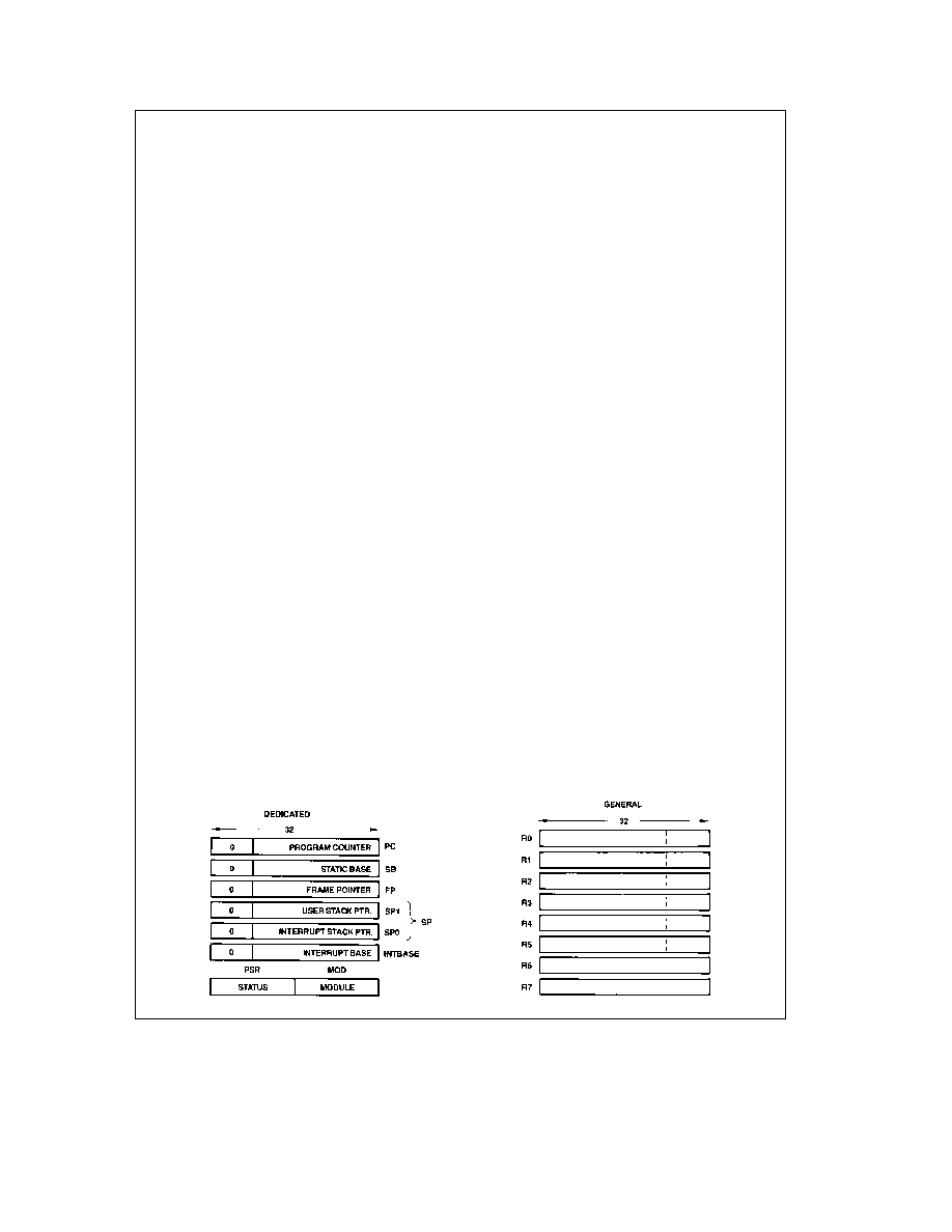
2 1 1 General Purpose Registers
There are eight registers for meeting high speed general
storage requirements such as holding temporary variables
and addresses The general purpose registers are free for
any use by the programmer They are thirty-two bits in
length If a general register is specified for an operand that
is eight or sixteen bits long only the low part of the register
is used the high part is not referenced or modified
2 1 2 Dedicated Registers
The eight dedicated registers of the NS32C016 are as-
signed specific functions
PC
The PROGRAM COUNTER register is a pointer to the
first byte of the instruction currently being executed The PC
is used to reference memory in the program section (In the
NS32C016 the upper eight bits of this register are always
zero )
SP0 SP1
The SP0 register points to the lowest address of
the last item stored on the INTERRUPT STACK This stack
is normally used only by the operating system It is used
primarily for storing temporary data and holding return infor-
mation for operating system subroutines and interrupt and
TL EE 8525 � 3
FIGURE 2-1 The General and Dedicated Registers
5
2 0 Architectural Description
(Continued)
trap service routines The SP1 register points to the lowest
address of the last item stored on the USER STACK This
stack is used by normal user programs to hold temporary
data and subroutine return information
In this document reference is made to the SP register The
terms ``SP register'' or ``SP'' refer to either SP0 or SP1
depending on the setting of the S bit in the PSR register If
the S bit in the PSR is 0 then SP refers to SP0 If the S bit in
the PSR is 1 then SP refers to SP1 (In the NS32C016 the
upper eight bits of these registers are always zero )
Stacks in the Series 32000 family grow downward in memo-
ry A Push operation pre-decrements the Stack Pointer by
the operand length A Pop operation post-increments the
Stack Pointer by the operand length
FP
The FRAME POINTER register is used by a procedure
to access parameters and local variables on the stack The
FP register is set up on procedure entry with the ENTER
instruction and restored on procedure termination with the
EXIT instruction
The frame pointer holds the address in memory occupied by
the old contents of the frame pointer (In the NS32C016 the
upper eight bits of this register are always zero )
SB
The STATIC BASE register points to the global vari-
ables of a software module This register is used to support
relocatable global variables for software modules The SB
register holds the lowest address in memory occupied by
the global variables of a module (In the NS32C016 the up-
per eight bits of this register are always zero )
INTBASE
The INTERRUPT BASE register holds the ad-
dress of the dispatch table for interrupts and traps (Section
3 8) The INTBASE register holds the lowest address in
memory occupied by the dispatch table (In the NS32C016
the upper eight bits of this register are always zero )
MOD
The MODULE register holds the address of the mod-
ule descriptor of the currently executing software module
The MOD register is sixteen bits long therefore the module
table must be contained within the first 64k bytes of memo-
ry
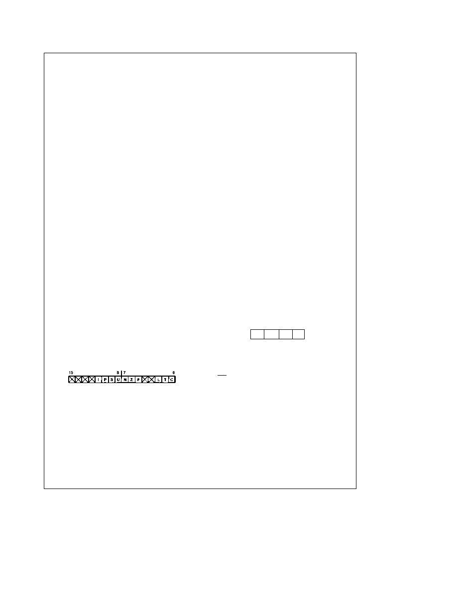
PSR
The PROCESSOR STATUS REGISTER (PSR) holds
the status codes for the NS32C016 microprocessor
The PSR is sixteen bits long divided into two eight-bit
halves The low order eight bits are accessible to all pro-
grams but the high order eight bits are accessible only to
programs executing in Supervisor Mode
TL EE 8525 � 78
FIGURE 2-2 Processor Status Register
C
The C bit indicates that a carry or borrow occurred after
an addition or subtraction instruction It can be used with the
ADDC and SUBC instructions to perform multiple-precision
integer arithmetic calculations It may have a setting of 0 (no
carry or borrow) or 1 (carry or borrow)
T
The T bit causes program tracing If this bit is a 1 a TRC
trap is executed after every instruction (Section 3 8 5)
L
The L bit is altered by comparison instructions In a com-
parison instruction the L bit is set to ``1'' if the second oper-
and is less than the first operand when both operands are
interpreted as unsigned integers Otherwise it is set to ``0''
In Floating Point comparisons this bit is always cleared
F
The F bit is a general condition flag which is altered by
many instructions (e g integer arithmetic instructions use it
to indicate overflow)
Z
The Z bit is altered by comparison instructions In a com-
parison instruction the Z bit is set to ``1'' if the second oper-
and is equal to the first operand otherwise it is set to ``0''
N
The N bit is altered by comparison instructions In a com-
parison instruction the N bit is set to ``1'' if the second oper-
and is less than the first operand when both operands are
interpreted as signed integers Otherwise it is set to ``0''
U
If the U bit is ``1'' no privileged instructions may be exe-
cuted If the U bit is ``0'' then all instructions may be execut-
ed When U
e
0 the NS32C016 is said to be in Supervisor
Mode when U
e
1 the NS32C016 is said to be in User
Mode A User Mode program is restricted from executing
certain instructions and accessing certain registers which
could interfere with the operating system For example a
User Mode program is prevented from changing the setting
of the flag used to indicate its own privilege mode A Super-
visor Mode program is assumed to be a trusted part of the
operating system hence it has no such restrictions
S
The S bit specifies whether the SP0 register or SP1 regis-
ter is used as the stack pointer The bit is automatically
cleared on interrupts and traps It may have a setting of 0
(use the SP0 register) or 1 (use the SP1 register)
P
The P bit prevents a TRC trap from occurring more than
once for an instruction (Section 3 8 5) It may have a setting
of 0 (no trace pending) or 1 (trace pending)
I
If I
e
1 then all interrupts will be accepted (Section 3 8) If
I
e
0 only the NMI interrupt is accepted Trap enables are
not affected by this bit
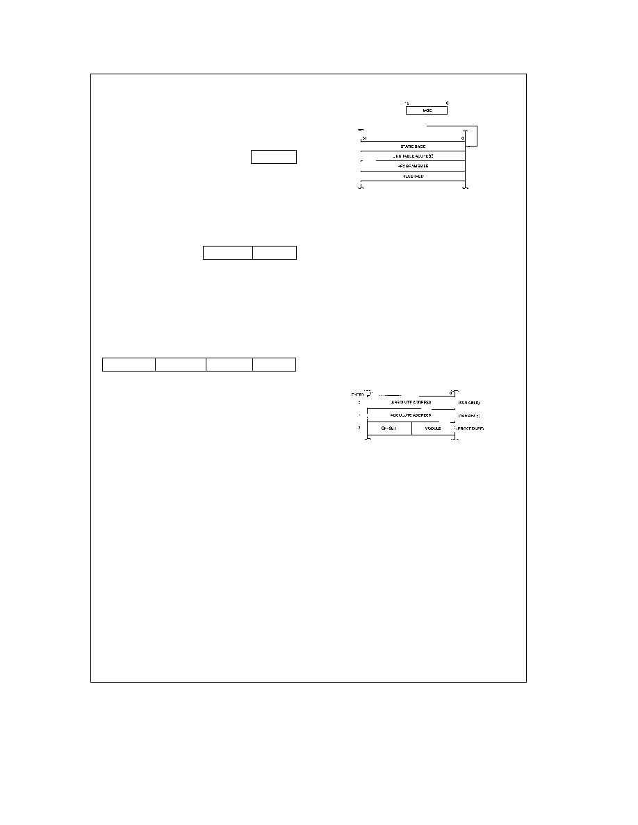
2 1 3 The Configuration Register (CFG)
Within the Control section of the NS32C016 CPU is the four-
bit CFG Register which declares the presence of certain
external devices It is referenced by only one instruction
SETCFG which is intended to be executed only as part of
system initialization after reset The format of the CFG Reg-
ister is shown in
Figure 2-3
C
M
F
I
FIGURE 2-3 CFG Register
The CFG I bit declares the presence of external interrupt
vectoring circuitry (specifically the NS32202 Interrupt Con-
trol Unit) If the CFG I bit is set interrupts requested through
the INT pin are ``Vectored '' If it is clear these interrupts are
``Non-Vectored '' See Section 3 8
The F M and C bits declare the presence of the FPU MMU
and Custom Slave Processors If these bits are not set the
corresponding instructions are trapped as being undefined
2 1 4 Memory Organization
The main memory of the NS32C016 is a uniform linear ad-
dress space Memory locations are numbered sequentially
starting at zero and ending at 2
24
1 The number specify-
ing a memory location is called an address The contents of
each memory location is a byte consisting of eight bits Un-
less otherwise noted diagrams in this document show data
stored in memory with the lowest address on the right and
the highest address on the left Also when data is shown
vertically the lowest address is at the top of a diagram and
6
2 0 Architectural Description
(Continued)
the highest address at the bottom of the diagram When bits
are numbered in a diagram the least significant bit is given
the number zero and is shown at the right of the diagram
Bits are numbered in increasing significance and toward the
left
7
0
A
Byte at Address A
Two contiguous bytes are called a word Except where not-
ed (Section 2 2 1) the least significant byte of a word is
stored at the lower address and the most significant byte of
the word is stored at the next higher address In memory
the address of a word is the address of its least significant
byte and a word may start at any address
15 MSB's 8 7 LSB's 0
A
a
1
A
Word at Address A
Two contiguous words are called a double word Except
where noted (Section 2 2 1) the least significant word of a
double word is stored at the lowest address and the most
significant word of the double word is stored at the address
two greater In memory the address of a double word is the
address of its least significant byte and a double word may
start at any address
31 MSB's 24 23
16 15
8 7 LSB's 0
A
a
3
A
a
2
A
a
1
A
Double Word at Address A
Although memory is addressed as bytes it is actually orga-
nized as words Therefore words and double words that are
aligned to start at even addresses (multiples of two) are
accessed more quickly than words and double words that
are not so aligned
2 1 5 Dedicated Tables
Two of the NS32C016 dedicated registers (MOD and INT-
BASE) serve as pointers to dedicated tables in memory
The INTBASE register points to the Interrupt Dispatch and
Cascade tables These are described in Section 3 8
The MOD register contains a pointer into the Module Table
whose entries are called Module Descriptors A Module De-
scriptor contains four pointers three of which are used by
the NS32C016 The MOD register contains the address of
the Module Descriptor for the currently running module It is
automatically updated by the Call External Procedure in-
structions (CXP and CXPD)
The format of a Module Descriptor is shown in
Figure 2-4
The Static Base entry contains the address of static data
assigned to the running module It is loaded into the CPU
Static Base register by the CXP and CXPD instructions The
Program Base entry contains the address of the first byte of
instruction code in the module Since a module may have
multiple entry points the Program Base pointer serves only
as a reference to find them
TL EE 8525 � 4
FIGURE 2-4 Module Descriptor Format
The Link Table Address points to the Link Table for the
currently running module The Link Table provides the infor-
mation needed for
1)
Sharing variables between modules Such variables
are accessed through the Link Table via the External
addressing mode
2)
Transferring control from one module to another This
is done via the Call External Procedure (CXP) instruc-
tion
The format of a Link Table is given in
Figure 2-5 A Link
Table Entry for an external variable contains the 32-bit ad-
dress of that variable An entry for an external procedure
contains two 16-bit fields Module and Offset The Module
field contains the new MOD register contents for the mod-
ule being entered The Offset field is an unsigned number
giving the position of the entry point relative to the new
module's Program Base pointer
For further details of the functions of these tables see the
Series 32000 Instruction Set Reference Manual
TL EE 8525 � 5
FIGURE 2-5 A Sample Link Table
2 2 INSTRUCTION SET
2 2 1 General Instruction Format
Figure 2-6 shows the general format of a Series 32000 in-
struction The Basic Instruction is one to three bytes long
and contains the Opcode and up to 5-bit General Address-
ing Mode (``Gen'') fields Following the Basic Instruction
field is a set of optional extensions which may appear de-
pending on the instruction and the addressing modes se-
lected
Index Bytes appear when either or both Gen fields specify
Scaled Index In this case the Gen field specifies only the
Scale Factor (1 2 4 or 8) and the Index Byte specifies
which General Purpose Register to use as the index and
which addressing mode calculation to perform before index-
ing See
Figure 2-7
Following Index Bytes come any displacements (addressing
constants) or immediate values associated with the select-
ed addressing modes Each Disp lmm field may contain
7

2 0 Architectural Description
(Continued)
TL EE 8525 � 6
FIGURE 2-6 General Instruction Format
TL EE 8525 � 7
FIGURE 2-7 Index Byte Format
one of two displacements or one immediate value The size
of a Displacement field is encoded within the top bits of that
field as shown in
Figure 2-8 with the remaining bits inter-
preted as a signed (two's complement) value The size of an
immediate value is determined from the Opcode field Both
Displacement and Immediate fields are stored most-signifi-
cant byte first Note that this is different from the memory
representation of data (Section 2 1 4)
Some instructions require additional ``implied'' immediates
and or displacements apart from those associated with ad-
dressing modes Any such extensions appear at the end of
the instruction in the order that they appear within the list of
operands in the instruction definition (Section 2 2 3)
2 2 2 Addressing Modes
The NS32C016 CPU generally accesses an operand by cal-
culating its Effective Address based on information avail-
able when the operand is to be accessed The method to be
used in performing this calculation is specified by the pro-
grammer as an ``addressing mode ''
Addressing modes in the NS32C016 are designed to opti-
mally support high-level language accesses to variables In
nearly all cases a variable access requires only one ad-
dressing mode within the instruction that acts upon that
variable Extraneous data movement is therefore minimized
NS32C016 Addressing Modes fall into nine basic types
Register
The operand is available in one of the eight Gen-
eral Purpose Registers In certain Slave Processor instruc-
tions an auxiliary set of eight registers may be referenced
instead
Register Relative
A General Purpose Register contains an
address to which is added a displacement value from the
instruction yielding the Effective Address of the operand in
memory
Memory Space
Identical to Register Relative above ex-
cept that the register used is one of the dedicated registers
PC SP SB or FP These registers point to data areas gen-
erally needed by high-level languages
Memory Relative
A pointer variable is found within the
memory space pointed to by the SP SB or FP register A
Byte Displacement Range
b
64 to
a
63
Word Displacement Range
b
8192 to
a
8191
Double Word Displacement
Range (Entire Addressing Space)
TL EE 8525 � 8
FIGURE 2-8 Displacement Encodings
displacement is added to that pointer to generate the Effec-
tive Address of the operand
Immediate
The operand is encoded within the instruction
This addressing mode is not allowed if the operand is to be
written
Absolute
The address of the operand is specified by a
displacement field in the instruction
External
A pointer value is read from a specified entry of
the current Link Table To this pointer value is added a dis-
placement yielding the Effective Address of the operand
Top of Stack
The currently-selected Stack Pointer (SP0 or
SP1) specifies the location of the operand The operand is
pushed or popped depending on whether it is written or
read
8

2 0 Architectural Description
(Continued)
Scaled Index
Although encoded as an addressing mode
Scaled Indexing is an option on any addressing mode ex-
cept Immediate or another Scaled Index It has the effect of
calculating an Effective Address then multiplying any Gen-
eral Purpose Register by 1 2 4 or 8 and adding into the
total yielding the final Effective Address of the operand
Table 2-1 is a brief summary of the addressing modes For a
complete description of their actions see the Series 32000
Instruction Set Reference Manual
TABLE 2-1 NS32C016 Addressing Modes
ENCODING
MODE
ASSEMBLER SYNTAX
EFFECTIVE ADDRESS
Register
00000
Register 0
R0 or F0
None Operand is in the specified
00001
Register 1
R1 or F1
register
00010
Register 2
R2 or F2
00011
Register 3
R3 or F3
00100
Register 4
R4 or F4
00101
Register 5
R5 or F5
00110
Register 6
R6 or F6
00111
Register 7
R6 or F7
Register Relative
01000
Register 0 relative
disp(R0)
Disp
a
Register
01001
Register 1 relative
disp(R1)
01010
Register 2 relative
disp(R2)
01011
Register 3 relative
disp(R3)
01100
Register 4 relative
disp(R4)
01101
Register 5 relative
disp(R5)
01110
Register 6 relative
disp(R6)
01111
Register 7 relative
disp(R7)
Memory Relative
10000
Frame memory relative
disp2(disp1 (FP))
Disp2
a
Pointer Pointer found at
10001
Stack memory relative
disp2(disp1 (SP))
address Disp 1
a
Register ``SP''
10010
Static memory relative
disp2(disp1 (SB))
is either SP0 or SP1 as selected
in PSR
Reserved
10011
(Reserved for Future Use)
Immediate
10100
Immediate
value
None Operand is input from
instruction queue
Absolute
10101
Absolute
disp
Disp
External
10110
External
EXT (disp1)
a
disp2
Disp2
a
Pointer Pointer is found
at Link Table Entry number Disp1
Top Of Stack
10111
Top of stack
TOS
Top of current stack using either
User or Interrupt Stack Pointer
as selected in PSR Automatic
Push Pop included
Memory Space
11000
Frame memory
disp(FP)
Disp
a
Register ``SP'' is either
11001
Stack memory
disp(SP)
SP0 or SP1 as selected in PSR
11010
Static memory
disp(SB)
11011
Program memory
a
disp
Scaled Index
11100
Index bytes
mode Rn B
EA (mode)
a
Rn
11101
Index words
mode Rn W
EA (mode)
a
2
c
Rn
11110
Index double words
mode Rn D
EA (mode)
a
4
c
Rn
11111
Index quad words
mode Rn Q
EA (mode)
a
8
c
Rn
``Mode'' and ``n'' are contained
within the Index Byte
EA (mode) denotes the effective
address generated using mode
9

2 0 Architectural Description
(Continued)
2 2 3 Instruction Set Summary
Table 2-2 presents a brief description of the NS32C016 in-
struction set The Format column refers to the Instruction
Format tables (Appendix A) The Instruction column gives
the instruction as coded in assembly language and the De-
scription column provides a short description of the function
provided by that instruction Further details of the exact op-
erations performed by each instruction may be found in the
Series 32000 Instruction Set Reference Manual
Notations
i
e
Integer length suffix B
e
Byte
W
e
Word
D
e
Double Word
f
e
Floating Point length suffix F
e
Standard Floating
L
e
Long Floating
gen
e
General operand Any addressing mode can be speci-
fied
short
e
A 4-bit value encoded within the Basic Instruction
(see Appendix A for encodings)
imm
e
Implied immediate operand An 8-bit value appended
after any addressing extensions
disp
e
Displacement (addressing constant) 8 16 or 32 bits
All three lengths legal
reg
e
Any General Purpose Register R0 � R7
areg
e
Any Dedicated Address Register SP SB FP MOD
INTBASE PSR US (bottom 8 PSR bits)
mreg
e
Any Memory Management Status Control Register
creg
e
A Custom Slave Processor Register (Implementation
Dependent)
cond
e
Any condition code encoded as a 4-bit field within
the Basic Instruction (see Appendix A for encodings)
TABLE 2-2 NS32C016 Instruction Set Summary
MOVES
Format
Operation
Operands
Description
4
MOVi
gen gen
Move a value
2
MOVQi
short gen
Extend and move a signed 4-bit constant
7
MOVMi
gen gen disp
Move multiple disp bytes (1 to 16)
7
MOVZBW
gen gen
Move with zero extension
7
MOVZiD
gen gen
Move with zero extension
7
MOVXBW
gen gen
Move with sign extension
7
MOVXiD
gen gen
Move with sign extension
4
ADDR
gen gen
Move effective address
INTEGER ARITHMETIC
Format
Operation
Operands
Description
4
ADDi
gen gen
Add
2
ADDQi
short gen
Add signed 4-bit constant
4
ADDCi
gen gen
Add with carry
4
SUBi
gen gen
Subtract
4
SUBCi
gen gen
Subtract with carry (borrow)
6
NEGi
gen gen
Negate (2's complement)
6
ABSi
gen gen
Take absolute value
7
MULi
gen gen
Multiply
7
QUOi
gen gen
Divide rounding toward zero
7
REMi
gen gen
Remainder from QUO
7
DIVi
gen gen
Divide rounding down
7
MODi
gen gen
Remainder from DIV (Modulus)
7
MEIi
gen gen
Multiply to extended integer
7
DEIi
gen gen
Divide extended integer
PACKED DECIMAL (BCD) ARITHMETIC
Format
Operation
Operands
Description
6
ADDPi
gen gen
Add packed
6
SUBPi
gen gen
Subtract packed
10

2 0 Architectural Description
(Continued)
TABLE 2-2 NS32C016 Instruction Set Summary
(Continued)
INTEGER COMPARISON
Format
Operation
Operands
Description
4
CMPi
gen gen
Compare
2
CMPQi
short gen
Compare to signed 4-bit constant
7
CMPMi
gen gen disp
Compare multiple disp bytes (1 to 16)
LOGICAL AND BOOLEAN
Format
Operation
Operands
Description
4
ANDi
gen gen
Logical AND
4
ORi
gen gen
Logical OR
4
BICi
gen gen
Clear selected bits
4
XORi
gen gen
Logical exclusive OR
6
COMi
gen gen
Complement all bits
6
NOTi
gen gen
Boolean complement LSB only
2
Scondi
gen
Save condition code (cond) as a Boolean variable of size i
SHIFTS
Format
Operation
Operands
Description
6
LSHi
gen gen
Logical shift left or right
6
ASHi
gen gen
Arithmetic shift left or right
6
ROTi
gen gen
Rotate left or right
BITS
Format
Operation
Operands
Description
4
TBITi
gen gen
Test bit
6
SBITi
gen gen
Test and set bit
6
SBITIi
gen gen
Test and set bit interlocked
6
CBITi
gen gen
Test and clear bit
6
CBITIi
gen gen
Test and clear bit interlocked
6
IBITi
gen gen
Test and invert bit
8
FFSi
gen gen
Find first set bit
BIT FIELDS
Bit fields are values in memory that are not aligned to byte boundaries Examples are PACKED arrays and records used in
Pascal ``Extract'' instructions read and align a bit field ``Insert'' instructions write a bit field from an aligned source
Format
Operation
Operands
Description
8
EXTi
reg gen gen disp
Extract bit field (array oriented)
8
INSi
reg gen gen disp
Insert bit field (array oriented)
7
EXTSi
gen gen imm imm
Extract bit field (short form)
7
INSSi
gen gen imm imm
Insert bit field (short form)
8
CVTP
reg gen gen
Convert to bit field pointer
ARRAYS
Format
Operation
Operands
Description
8
CHECKi
reg gen gen
Index bounds check
8
INDEXi
reg gen gen
Recursive indexing step for multiple-dimensional arrays
11

2 0 Architectural Description
(Continued)
TABLE 2-2 NS32C016 Instruction Set Summary
(Continued)
STRINGS
String instructions assign specific functions to the General
Purpose Registers
R4
Comparison Value
R3
Translation Table Pointer
R2
String 2 Pointer
R1
String 1 Pointer
R0
Limit Count
Options on all string instructions are
B
(Backward)
Decrement strong pointers after each
step rather than incrementing
U
(Until match)
End instruction if String 1 entry matches
R4
W
(While match)
End instruction if String 1 entry does not
match R4
All string instructions end when R0 decrements to zero
Format
Operation
Operands
Description
5
MOVSi
options
Move string 1 to string 2
MOVST
options
Move string translating bytes
5
CMPSi
options
Compare string 1 to string 2
CMPST
options
Compare translating string 1 bytes
5
SKPSi
options
Skip over string 1 entries
SKPST
options
Skip translating bytes for until while
JUMPS AND LINKAGE
Format
Operation
Operands
Description
3
JUMP
gen
Jump
0
BR
disp
Branch (PC Relative)
0
Bcond
disp
Conditional branch
3
CASEi
gen
Multiway branch
2
ACBi
short gen disp
Add 4-bit constant and branch if non-zero
3
JSR
gen
Jump to subroutine
1
BSR
disp
Branch to subroutine
1
CXP
disp
Call external procedure
3
CXPD
gen
Call external procedure using descriptor
1
SVC
Supervisor call
1
FLAG
Flag trap
1
BPT
Breakpoint trap
1
ENTER
reg list disp
Save registers and allocate stack frame (Enter Procedure)
1
EXIT
reg list
Restore registers and reclaim stack frame (Exit Procedure)
1
RET
disp
Return from subroutine
1
RXP
disp
Return from external procedure call
1
RETT
disp
Return from trap (Privileged)
1
RETI
Return from interrupt (Privileged)
CPU REGISTER MANIPULATION
Format
Operation
Operands
Description
1
SAVE
reg list
Save general purpose registers
1
RESTORE
reg list
Restore general purpose registers
2
LPRi
areg gen
Load dedicated register (Privileged if PSR or INTBASE)
2
SPRi
areg gen
Store dedicated register (Privileged if PSR or INTBASE)
3
ADJSPi
gen
Adjust stack pointer
3
BISPSRi
gen
Set selected bits in PSR (Privileged if not Byte length)
3
BICPSRi
gen
Clear selected bits in PSR (Privileged if not Byte length)
5
SETCFG
option list
Set configuration register (Privileged)
12

2 0 Architectural Description
(Continued)
TABLE 2-2 NS32C016 Instruction Set Summary
(Continued)
FLOATING POINT
Format
Operation
Operands
Description
11
MOVf
gen gen
Move a floating point value
9
MOVLF
gen gen
Move and shorten a long value to standard
9
MOVFL
gen gen
Move and lengthen a standard value to long
9
MOVif
gen gen
Convert any integer to standard or long floating
9
ROUNDfi
gen gen
Convert to integer by rounding
9
TRUNCfi
gen gen
Convert to integer by truncating toward zero
9
FLOORfi
gen gen
Convert to largest integer less than or equal to value
11
ADDf
gen gen
Add
11
SUBf
gen gen
Subtract
11
MULf
gen gen
Multiply
11
DIVf
gen gen
Divide
11
CMPf
gen gen
Compare
11
NEGf
gen gen
Negate
11
ABSf
gen gen
Take absolute value
9
LFSR
gen
Load FSR
9
SFSR
gen
Store FSR
MEMORY MANAGEMENT
Format
Operation
Operands
Description
14
LMR
mreg gen
Load memory management register (Privileged)
14
SMR
mreg gen
Store memory management register (Privileged)
14
RDVAL
gen
Validate address for reading (Privileged)
14
WRVAL
gen
Validate address for writing (Privileged)
8
MOVSUi
gen gen
Move a value from supervisor
space to user space (Privileged)
8
MOVUSi
gen gen
Move a value from user space
to supervisor space (Privileged)
MISCELLANEOUS
Format
Operation
Operands
Description
1
NOP
No operation
1
WAIT
Wait for interrupt
1
DIA
Diagnose Single-byte ``Branch to Self'' for hardware
breakpointing Not for use in programming
CUSTOM SLAVE
Format
Operation
Operands
Description
15 5
CCAL0c
gen gen
Custom calculate
15 5
CCAL1c
gen gen
15 5
CCAL2c
gen gen
15 5
CCAL3c
gen gen
15 5
CMOV0c
gen gen
Custom move
15 5
CMOV1c
gen gen
15 5
CMOV2c
gen gen
15 5
CMOV3c
gen gen
15 5
CCMP0c
gen gen
Custom compare
15 5
CCMP1c
gen gen
15 1
CCV0ci
gen gen
Custom convert
15 1
CCV1ci
gen gen
15 1
CCV2ci
gen gen
15 1
CCV3ic
gen gen
15 1
CCV4DQ
gen gen
15 1
CCV5QD
gen gen
15 1
LCSR
gen
Load custom status register
15 1
SCSR
gen
Store custom status register
15 0
CATST0
gen
Custom address test (Privileged)
15 0
CATST1
gen
(Privileged)
15 0
LCR
creg gen
Load custom register (Privileged)
15 0
SCR
creg gen
Store custom register (Privileged)
13
3 0 Functional Description
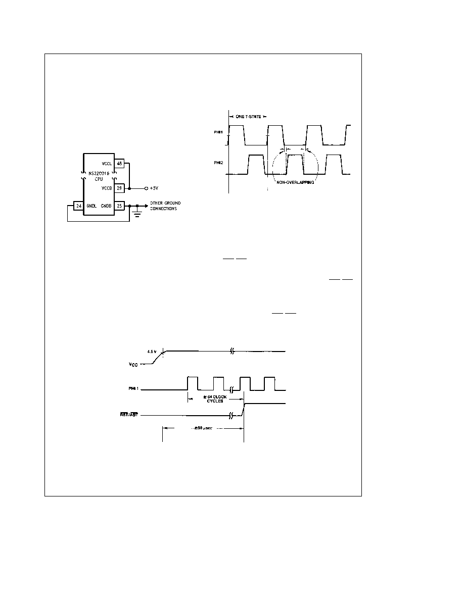
3 1 POWER AND GROUNDING
Power and ground connections for the NS32C016 are made
on four pins On-chip logic is connected to power through
the logic power pin (VCCL pin 48) and to ground through
the logic ground pin (GNDL pin 24) On-chip output drivers
are connected to power through the buffer power pin
(VCCP pin 29) and to ground through the buffer ground pin
(GNDB pin 25) For optimal noise immunity it is recom-
mended that single conductors be connected directly from
VCCL to VCCB and from GNDL to GNDB as shown below
(
Figure 3-1 )
TL EE 8525 � 9
FIGURE 3-1 Recommended Supply Connections
3 2 CLOCKING
The NS32C016 inputs clocking signals from the NS32C201
Timing Control Unit (TCU) which presents two non-overlap-
ping phases of a single clock frequency These phases are
called PHI1 (pin 26) and PHI2 (pin 27) Their relationship to
each other is shown in
Figure 3-2
Each rising edge of PHI1 defines a transition in the timing
state (``T-State'') of the CPU One T-State represents the
execution of one microinstruction within the CPU and or
one step of an external bus transfer See Section 4 for com-
plete specifications of PHI1 and PHI2
TL EE 8525 � 10
FIGURE 3-2 Clock Timing Relationships
As the TCU presents signals with very fast transitions it is
recommended that the conductors carrying PHI1 and PHI2
be kept as short as possible and that they not be connect-
ed anywhere except from the TCU to the CPU and if pres-
ent the MMU A TTL Clock signal (CTTL) is provided by the
TCU for all other clocking
3 3 RESETTING
The RST ABT pin serves both as a Reset for on-chip logic
and as the Abort input for Memory-Managed systems For
its use as the Abort Command see Section 3 5 4
The CPU may be reset at any time by pulling the RST ABT
pin low for at least 64 clock cycles Upon detecting a reset
the CPU terminates instruction processing resets its inter-
nal logic and clears the Program Counter (PC) and Proces-
sor Status Register (PSR) to all zeroes
On application of power RST ABT must be held low for at
least 50 ms after V
CC
is stable This is to ensure that all on-
chip voltages are completely stable before operation
Whenever a Reset is applied it must also remain active
TL EE 8525 � 11
FIGURE 3-3 Power-On Reset Requirements
14
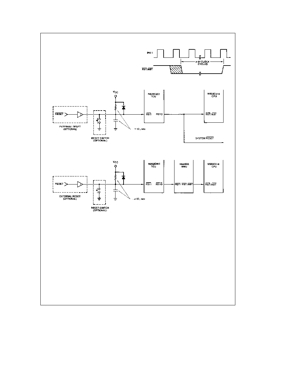
3 0 Functional Description
(Continued)
for not less than 64 clock cycles The rising edge must oc-
cur while PHI1 is high See
Figures 3-3 and 3-4
The NS32C201 Timing Control Unit (TCU) provides circuitry
to meet the Reset requirements of the NS32C016 CPU
Fig-
ure 3-5a shows the recommended connections for a non-
Memory-Managed system
Figure 3-5b shows the connec-
tions for a Memory-Managed system
TL EE 8525 � 12
FIGURE 3-4 General Reset Timing
TL EE 8525 � 13
FIGURE 3-5a Recommended Reset Connections Non-Memory-Managed System
TL EE 8525 � 14
FIGURE 3-5b Recommended Reset Connections Memory-Managed System
3 4 BUS CYCLES
The NS32C016 CPU has a strap option which defines the
Bus Timing Mode as either With or Without Address Trans-
lation This section describes only bus cycles under the No
Address Translation option For details of the use of the
strap and of bus cycles with address translation see Sec-
tion 3 5
The CPU will perform a bus cycle for one of the following
reasons
1) To write or read data to or from memory or a peripheral
interface device Peripheral input and output are memo-
ry-mapped in the Series 32000 family
2) To fetch instructions into the eight-byte instruction
queue This happens whenever the bus would otherwise
be idle and the queue is not already full
3) To acknowledge an interrupt and allow external circuitry
to provide a vector number or to acknowledge comple-
tion of an interrupt service routine
4) To transfer information to or from a Slave Processor
In terms of bus timing cases 1 through 3 above are identi-
cal For timing specifications see Section 4 The only exter-
nal difference between them is the four-bit code placed on
the Bus Status pins (ST0 � ST3) Slave Processor cycles dif-
fer in that separate control signals are applied (Section
3 4 6)
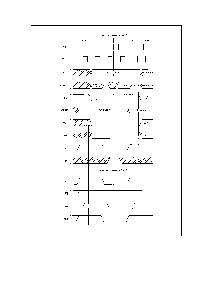
The sequence of events in a non-Slave bus cycle is shown
in
Figure 3-7 for a Read cycle and Figure 3-8 for a Write
cycle The cases shown assume that the selected memory
or interface device is capable of communicating with the
CPU at full speed If it is not then cycle extension may be
requested through the RDY line (Section 3 4 1)
15
3 0 Functional Description
(Continued)
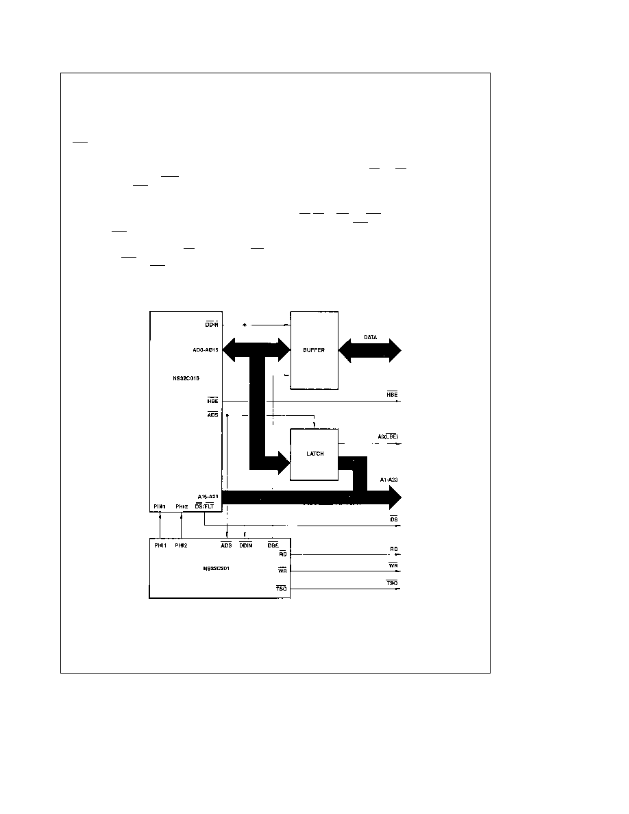
A full-speed bus cycle is performed in four cycles of the
PHI1 clock signal labeled T1 through T4 Clock cycles not
associated with a bus cycle are designated Ti (for ``Idle'')
During T1 the CPU applies an address on pins AD0 � AD15
and A16 � A23 It also provides a low-going pulse on the
ADS pin which serves the dual purpose of informing exter-
nal circuitry that a bus cycle is starting and of providing con-
trol to an external latch for demultiplexing Address bits 0 �
15 from the AD0 � AD15 pins See
Figure 3-6 During this
time also the status signals DDIN indicating the direction of
the transfer and HBE indicating whether the high byte
(AD8 � AD15) is to be referenced become valid
During T2 the CPU switches the Data Bus AD0 � AD15 to
either accept or present data Note that the signals A16 �
A23 remain valid and need not be latched It also starts the
data strobe (DS) signaling the beginning of the data trans-
fer Associated signals from the NS32C201 Timing Control
Unit are also activated at this time RD (Read Strobe) or WR
(Write Strobe) TSO (Timing State Output indicating that T2
has been reached) and DBE (Data Buffer Enable)
The T3 state provides for access time requirements and it
occurs at least once in a bus cycle At the end of T2 on the
falling edge of the PHI2 clock the RDY (Ready) line is sam-
pled to determine whether the bus cycle will be extended
(Section 3 4 1)
If the CPU is performing a Read cycle the Data Bus (AD0 �
AD15) is sampled at the falling edge of PHI2 of the last T3
state see Section 4 Data must however be held at least
until the beginning of T4 DS and RD are guaranteed not to
go inactive before this point so the rising edge of either of
them may safely be used to disable the device providing the
input data
The T4 state finishes the bus cycle At the beginning of T4
the DS RD or WR and TSO signals go inactive and at the
rising edge of PHI2 DBE goes inactive having provided for
necessary data hold times Data during Write cycles re-
mains valid from the CPU throughout T4 Note that the Bus
Status lines (ST0 � ST3) change at the beginning of T4 an-
ticipating the following bus cycle (if any)
TL EE 8525 � 15
FIGURE 3-6 Bus Connections
16
3 0 Functional Description
(Continued)
TL EE 8525 � 16
FIGURE 3-7 Read Cycle Timing
17
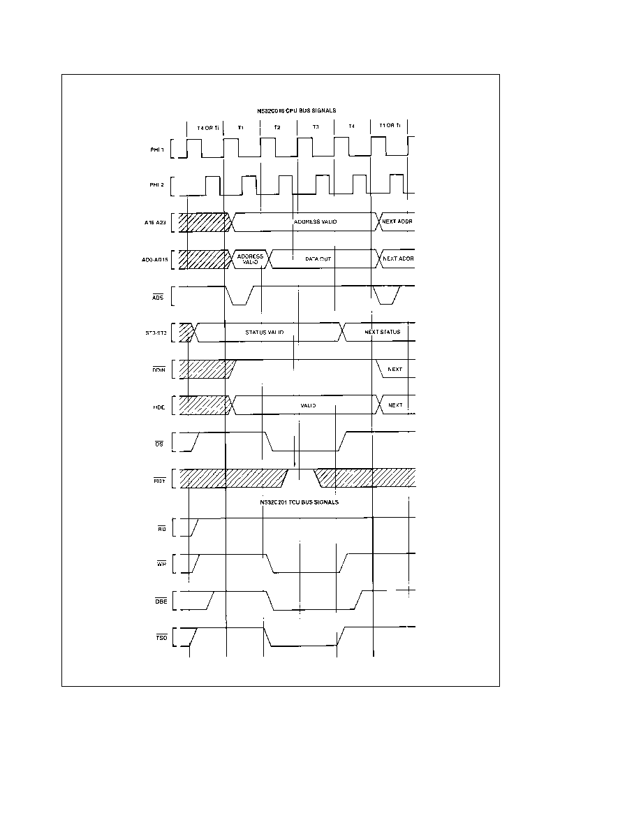
3 0 Functional Description
(Continued)
TL EE 8525 � 17
FIGURE 3-8 Write Cycle Timing
18
3 0 Functional Description
(Continued)
3 4 1 Cycle Extension
To allow sufficient strobe widths and access times for any
speed of memory or peripheral device the NS32C016 pro-
vides for extension of a bus cycle Any type of bus cycle
except a Slave Processor cycle can be extended
In
Figures 3-7 and 3-8 note that during T3 all bus control
signals from the CPU and TCU are flat Therefore a bus
cycle can be cleanly extended by causing the T3 state to be
repeated This is the purpose of the RDY (Ready) pin
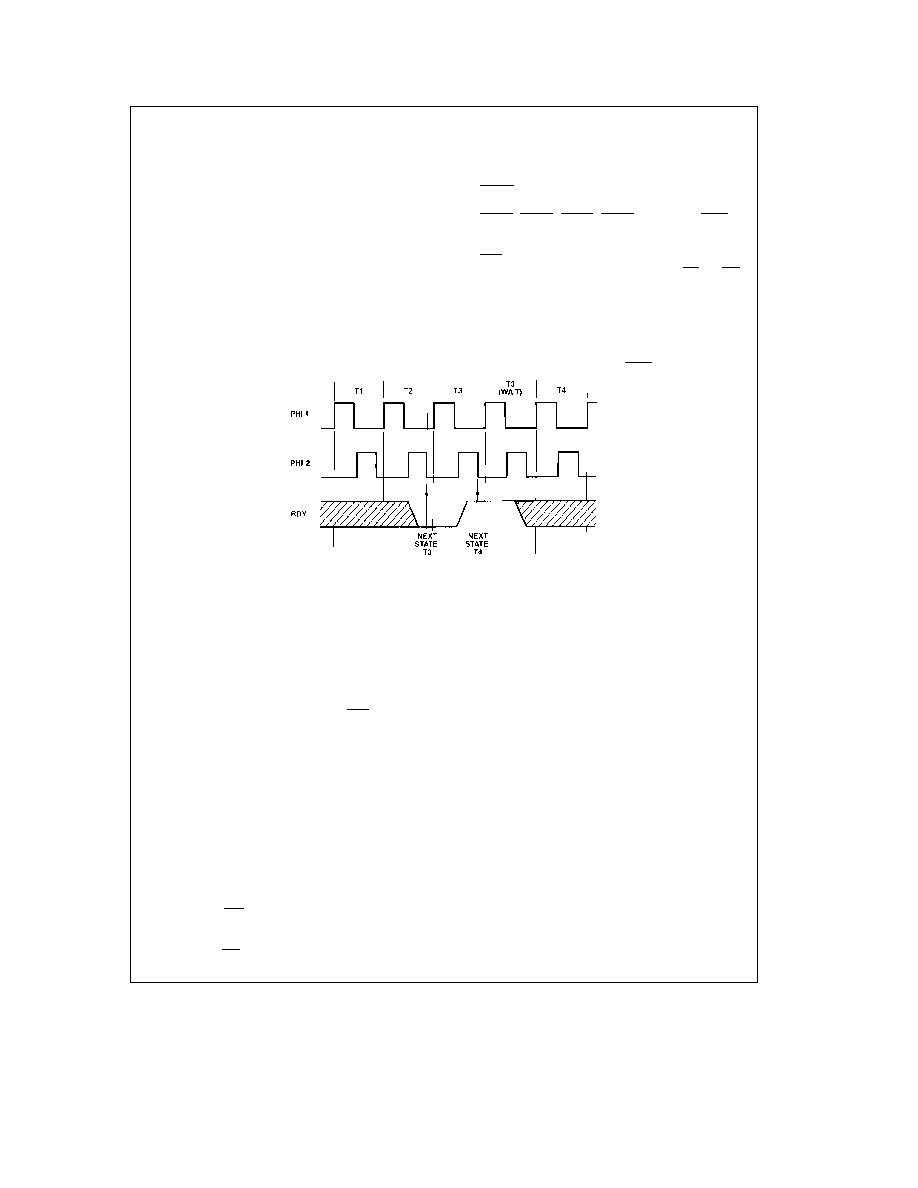
At the end of T2 on the falling edge of PHI2 the RDY line is
sampled by the CPU If RDY is high the next T-states will be
T3 and then T4 ending the bus cycle If it is sampled low
then another T3 state will be inserted after the next T-state
and the RDY line will again be sampled on the falling edge
of PHI2 Each additional T3 state after the first is referred to
as a ``wait state '' See
Figure 3-9
The RDY pin is driven by the NS32C201 Timing Control
Unit which applies WAIT States to the CPU as requested
on three sets of pins
1) CWAIT (Continues WAIT) which holds the CPU in WAIT
states until removed
2) WAIT1 WAIT2 WAIT4 WAIT8 (Collectively WAITn)
which may be given a four-bit binary value requesting a
specific number of WAIT States from 0 to 15
3) PER (Peripheral) which inserts five additional WAIT
states and causes the TCU to reshape the RD and WR
strobes This provides the setup and hold times required
by most MOS peripheral interface devices
Combinations of these various WAIT requests are both legal
and useful For details of their use see the NS32C201 TCU
Data Sheet
Figure 3-10 illustrates a typical Read cycle with two WAIT
states requested through the TCU WAITn pins
TL EE 8525 � 18
FIGURE 3-9 RDY Pin Timing
3 4 2 Bus Status
The NS32C016 CPU presents four bits of Bus Status infor-
mation on pins ST0 � ST3 The various combinations on
these pins indicate why the CPU is performing a bus cycle
or if it is idle on the bus then why it is idle
Referring to
Figures 3-7 and 3-8 note that Bus Status leads
the corresponding Bus Cycle going valid one clock cycle
before T1 and changing to the next state at T4 This allows
the system designer to fully decode the Bus Status and if
desired latch the decoded signals before ADS initiates the
Bus Cycle
The Bus Status pins are interpreted as a four-bit value with
ST0 the least significant bit Their values decode as follows
0000
The bus is idle because the CPU does not need
to perform a bus access
0001
The bus is idle because the CPU is executing
the WAIT instruction
0010
(Reserved for future use )
0011
The bus is idle because the CPU is waiting for a
Slave Processor to complete an instruction
0100
Interrupt Acknowledge Master
The CPU is performing a Read cycle To ac-
knowledge receipt of a Non-Maskable Interrupt
(on NMI) it will read from address FFFF00
16
but will ignore any data provided
To acknowledge receipt of a Maskable Interrupt
(on INT) it will read from address FFFE00
16
expecting a vector number to be provided from
the Master NS32202 Interrupt Control Unit If
the vectoring mode selected by the last
SETCFG instruction was Non-Vectored then
the CPU will ignore the value it has read and will
use a default vector instead having assumed
that no NS32202 is present See Section 3 4 5
0101
Interrupt Acknowledge Cascaded
The CPU is reading a vector number from a
Cascaded NS32202 Interrupt Control Unit The
address
provided
is
the
address
of
the
NS32202 Hardware Vector register See Sec-
tion 3 4 5
0110
End of Interrupt Master
The CPU is performing a Read cycle to indicate
that it is executing a Return from Interrupt
(RETI) instruction See Section 3 4 5
0111
End of Interrupt Cascaded
The CPU is reading from a Cascaded Interrupt
Control Unit to indicate that it is returning
(through RETI) from an interrupt service routine
requested by that unit See Section 3 4 5
1000
Sequential Instruction Fetch
The CPU is reading the next sequential word
from the instruction stream into the Instruction
Queue It will do so whenever the bus would
otherwise be idle and the queue is not already
full
19
3 0 Functional Description
(Continued)
TL EE 8525�19
FIGURE 3-10 Extended Cycle Example
Note
Arrows on CWAIT PER WAITn indicate points at which the TCU samples Arrows on AD0�AD15 and
RDY indicate points at which the CPU samples
20
3 0 Functional Description
(Continued)
1001
Non-Sequential Instruction Fetch
The CPU is performing the first fetch of instruc-
tion code after the Instruction Queue is purged
This will occur as a result of any jump or branch
or any interrupt or trap or execution of certain
instructions
1010
Data Transfer
The CPU is reading or writing an operand of an
instruction
1011
Read RMW Operand
The CPU is reading an operand which will sub-
sequently be modified and rewritten If memory
protection circuitry would not allow the following
Write cycle it must abort this cycle
1100
Read for Effective Address Calculation
The CPU is reading information from memory in
order to determine the Effective Address of an
operand This will occur whenever an instruc-
tion uses the Memory Relative or External ad-
dressing mode
1101
Transfer Slave Processor Operand
The CPU is either transferring an instruction op-
erand to or from a Slave Processor or it is issu-
ing the Operation Word of a Slave Processor
instruction See Section 3 9 1
1110
Read Slave Processor Status
The CPU is reading a Status Word from a Slave
Processor This occurs after the Slave Proces-
sor has signalled completion of an instruction
The transferred word tells the CPU whether a
trap should be taken and in some instructions it
presents new values for the CPU Processor
Status Register bits N Z L or F See Section
3 9 1
1111
Broadcast Slave ID
The CPU is initiating the execution of a Slave
Processor instruction The ID Byte (first byte of
the instruction) is sent to all Slave Processors
one of which will recognize it From this point
the CPU is communicating with only one Slave
Processor See Section 3 9 1
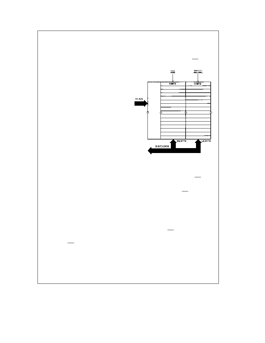
3 4 3 Data Access Sequences
The 24-bit address provided by the NS32C016 is a byte
address
that is
it uniquely identifies one of up to
16 777 216 eight-bit memory locations An important feature
of the NS32C016 is that the presence of a 16-bit data bus
imposes no restrictions on data alignment any data item
regardless of size may be placed starting at any memory
address The NS32C016 provides a special control signal
High Byte Enable (HBE) which facilitates individual byte ad-
dressing on a 16-bit bus
Memory is organized as two eight-bit banks each bank re-
ceiving the word address (A1 � A23) in parallel One bank
connected to Data Bus pins AD0 � AD7 is enabled to re-
spond to even byte addresses i e when the least signifi-
cant address bit (A0) is low The other bank connected to
Data Bus pins AD8 � AD15 is enabled when HBE is low See
Figure 3-11
TL EE 8525 � 20
FIGURE 3-11 Memory Interface
Any bus cycle falls into one of three categories Even Byte
Access Odd Byte Access and Even Word Access All ac-
cesses to any data type are made up of sequences of these
cycles Table 3-1 gives the state of A0 and HBE for each
category
TABLE 3-1 Bus Cycle Categories
Category
HBE
A0
Even Byte
1
0
Odd Byte
0
1
Even Word
0
0
Accesses of operands requiring more than one bus cycle
are performed sequentially with no idle T-States separating
them The number of bus cycles required to transfer an op-
erand depends on its size and its alignment (i e whether it
starts on an even byte address or an odd byte address)
Table 3-2 lists the bus cycle performed for each situation
For the timing of A0 and HBE see Section 3 4
21

3 0 Functional Description
(Continued)
TABLE 3-2 Access Sequences
Cycle
Type
Address
HBE
A0
High Bus
Low Bus
A Odd Word Access Sequence
BYTE 1
BYTE 0
w
A
1
Odd Byte
A
0
1
Byte 0
Don't Care
2
Even Byte
A
a
1
1
0
Don't Care
Byte 1
B Even Double-Word Access Sequence
BYTE 3
BYTE 2
BYTE 1
BYTE 0
w
A
1
Even Word
A
0
0
Byte 1
Byte 0
2
Even Word
A
a
2
0
0
Byte 3
Byte 2
C Odd Double-Word Access Sequence
BYTE 3
BYTE 2
BYTE 1
BYTE 0
w
A
1
Odd Byte
A
0
1
Byte 0
Don't Care
2
Even Word
A
a
1
0
0
Byte 2
Byte 1
3
Even Byte
A
a
3
1
0
Don't Care
Byte 3
D Even Quad-Word Access Sequence
BYTE 7
BYTE 6
BYTE 5
BYTE 4
BYTE 3
BYTE 2
BYTE 1
BYTE 0
w
A
1
Even Word
A
0
0
Byte 1
Byte 0
2
Even Word
A
a
2
0
0
Byte 3
Byte 2
Other bus cycles (instruction prefetch or slave) can occur here
3
Even Word
A
a
4
0
0
Byte 5
Byte 4
4
Even Word
A
a
6
0
0
Byte 7
Byte 6
E Odd Quad-Word Access Sequence
BYTE 7
BYTE 6
BYTE 5
BYTE 4
BYTE 3
BYTE 2
BYTE 1
BYTE 0
w
A
1
Odd Byte
A
0
1
Byte 0
Don't Care
2
Even Word
A
a
1
0
0
Byte 2
Byte 1
3
Even Byte
A
a
3
1
0
Don't Care
Byte 3
Other bus cycles (instruction prefetch or slave) can occur here
4
Odd Byte
A
a
4
0
1
Byte 4
Don't Care
5
Even Word
A
a
5
0
0
Byte 6
Byte 5
6
Even Byte
A
a
7
1
0
Don't Care
Byte 7
22

3 0 Functional Description
(Continued)
3 4 3 1 Bit Accesses
The Bit Instructions perform byte accesses to the byte con-
taining the designated bit The Test and Set Bit instruction
(SBIT) for example reads a byte alters it and rewrites it
having changed the contents of one bit
3 4 3 2 Bit Field Accesses
An access to a Bit Field in memory always generates a Dou-
ble-Word transfer at the address containing the least signifi-
cant bit of the field The Double Word is read by an Extract
instruction an Insert instruction reads a Double Word modi-
fies it and rewrites it
3 4 3 3 Extending Multiply Accesses
The Extending Multiply Instruction (MEI) will return a result
which is twice the size in bytes of the operand it reads If the
multiplicand is in memory the most-significant half of the
result is written first (at the higher address) then the least-
significant half This is done in order to support retry if this
instruction is aborted
3 4 4 Instruction Fetches
Instructions for the NS32C016 CPU are ``prefetched'' that
is they are input before being needed into the next available
entry of the eight-byte Instruction Queue The CPU performs
two types of Instruction Fetch cycles Sequential and Non-
Sequential These can be distinguished from each other by
their differing status combinations on pins ST0 � ST3 (Sec-
tion 3 4 2)
A Sequential Fetch will be performed by the CPU whenever
the Data Bus would otherwise be idle and the Instruction
Queue is not currently full Sequential Fetches are always
Even Word Read cycles (Table 3-1)
A Non-Sequential Fetch occurs as a result of any break in
the normally sequential flow of a program Any jump or
branch instruction a trap or an interrupt will cause the next
Instruction Fetch cycle to be Non-Sequential In addition
certain instructions flush the instruction queue causing the
next instruction fetch to display Non-Sequential status Only
the first bus cycle after a break displays Non-Sequential
status and that cycle is either an Even Word Read or an
Odd Byte Read depending on whether the destination ad-
dress is even or odd
3 4 5 Interrupt Control Cycles
Activating the INT or NMI pin on the CPU will initiate one or
more bus cycles whose purpose is interrupt control rather
than the transfer of instructions or data Execution of the
Return from Interrupt instruction (RETI) will also cause Inter-
rupt Control bus cycles These differ from instruction or data
transfers only in the status presented on pins ST0 � ST3 All
Interrupt Control cycles are single-byte Read cycles
This section describes only the Interrupt Control sequences
associated with each interrupt and with the return from its
service routine For full details of the NS32C016 interrupt
structure see Section 3 8
23

3 0 Functional Description
(Continued)
TABLE 3-3 Interrupt Sequences
Cycle
Status
Address
DDIN
HBE
A0
High Bus
Low Bus
A Non-Maskable Interrupt Control Sequences
Interrupt Acknowledge
1
0100
FFFF00
16
0
1
0
Don't Care
Don't Care
Interrupt Return
None Performed through Return from Trap (RETT) instruction
B Non-Vectored Interrupt Control Sequences
Interrupt Acknowledge
1
0100
FFFE00
16
0
1
0
Don't Care
Don't Care
Interrupt Return
None Performed through Return from Trap (RETT) instruction
C Vectored Interrupt Sequences Non-Cascaded
Interrupt Acknowledge
1
0100
FFFE00
16
0
1
0
Don't Care
Vector
Range 0 � 127
Interrupt Return
1
0110
FFFE00
16
0
1
0
Don't Care
Vector Same as
in Previous Int
Ack Cycle
D Vectored Interrupt Sequences Cascaded
Interrupt Acknowledge
1
0100
FFFE00
16
0
1
0
Don't Care
Cascade Index
range
b
16 to
b
1
(The CPU here uses the Cascade Index to find the Cascade Address )
2
0101
Cascade
0
1 or
0 or
Vector range 0 � 255 on appropriate
Address
0
1
half of Data Bus for even odd address
Interrupt Return
1
0110
FFFE00
16
0
1
0
Don't Care
Cascade Index
same as in
previous Int
Ack Cycle
(The CPU here uses the Cascade Index to find the Cascade Address )
2
0111
Cascade
0
1 or
0 or
Don't Care
Don't Care
Address
0
1
If the Cascaded ICU Address is Even (A0 is low) then the CPU applies HBE high and reads the vector number from bits 0�7 of the Data Bus
If the address is Odd (A0 is high) then the CPU applies HBE low and reads the vector number from bits 8�15 of the Data Bus The vector number may be in the
range 0�255
24
3 0 Functional Description
(Continued)
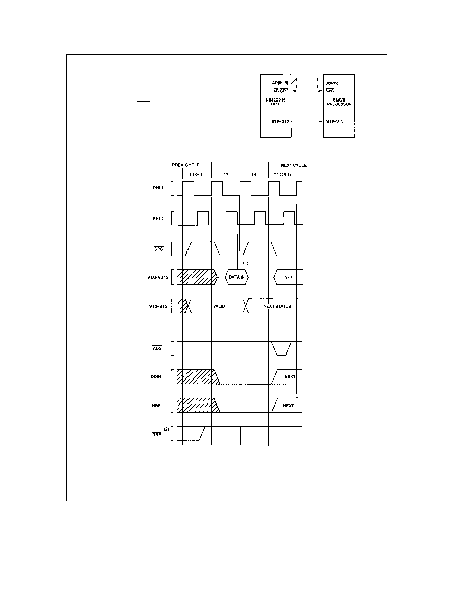
3 4 6 Slave Processor Communication
In addition to its use as the Address Translation strap (Sec-
tion 3 5 1) the AT SPC pin is used as the data strobe for
Slave Processor transfers In this role it is referred to as
Slave Processor Control (SPC) In a Slave Processor bus
cycle data is transferred on the Data Bus (AD0 � AD15) and
the status lines ST0 � ST3 are monitored by each Slave
Processor in order to determine the type of transfer being
performed SPC is bidirectional but is driven by the CPU
during all Slave Processor bus cycles See Section 3 9 for
full protocol sequences
TL EE 8525 � 21
FIGURE 3-12 Slave Processor Connections
TL EE 8525 � 22
Notes
(1) CPU samples Data Bus here
(2) DBE and all other NS32C201 TCU bus signals remain inactive because no ADS pulse is received from the CPU
FIGURE 3-13 CPU Read from Slave Processor
25
3 0 Functional Description
(Continued)
3 4 6 1 Slave Processor Bus Cycles
A Slave Processor bus cycle always takes exactly two clock
cycles labeled T1 and T4 (see
Figures 3-13 and 3-14 )
During a Read cycle SPC is active from the beginning of T1
to the beginning of T4 and the data is sampled at the end of
T1 The Cycle Status pins lead the cycle by one clock peri-
od and are sampled at the leading edge of SPC During a
Write cycle the CPU applies data and activates SPC at T1
removing SPC at T4 The Slave Processor latches status on
the leading edge of SPC and latches data on the trailing
edge
Since the CPU does not pulse the Address Strobe (ADS)
no bus signals are generated by the NS32C201 Timing Con-
trol Unit The direction of a transfer is determined by the
sequence (``protocol'') established by the instruction under
execution but the CPU indicates the direction on the DDIN
pin for hardware debugging purposes
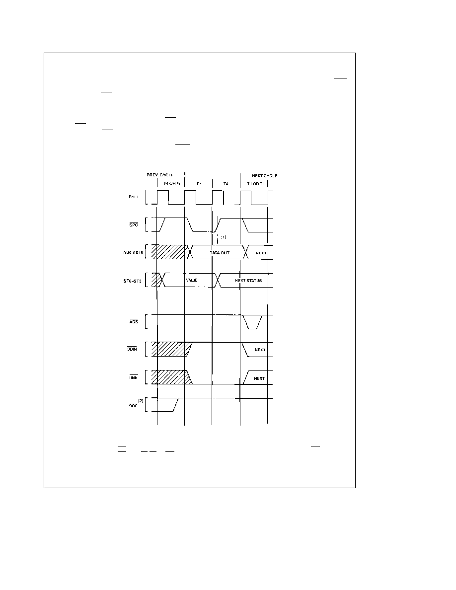
3 4 6 2 Slave Operand Transfer Sequences
A Slave Processor operand is transferred in one or more
Slave bus cycles A Byte operand is transferred on the
least-significant byte of the Data Bus (AD0 � AD7) and a
Word operand is transferred on the entire bus A Double
Word is transferred in a consecutive pair of bus cycles
least-significant word first A Quad Word is transferred in
two pairs of Slave cycles with other bus cycles possibly
occurring between them The word order is from least-signif-
icant word to most-significant
TL EE 8525 � 23
Notes
(1) Slave Processor samples Data Bus here
(2) DBE being provided by the NS32C201 TCU remains inactive due to the fact that no pulse is presented on ADS
TCU signals RD WR and TSO also remain inactive
FIGURE 3-14 CPU Write to Slave Processor
26

3 0 Functional Description
(Continued)
3 5 MEMORY MANAGEMENT OPTION
The NS32C016 CPU in conjunction with the NS32082
Memory Management Unit (MMU) provides full support for
address translation memory protection and memory alloca-
tion techniques up to and including Virtual Memory
3 5 1 Address Translation Strap
The Bus Interface Control section of the NS32C016 CPU
has two bus timing modes With or Without Address Trans-
lation The mode of operation is selected by the CPU by
sampling the AT SPC (Address Translation Slave Proces-
sor Control) pin on the rising edge of the RST (Reset) pulse
If AT SPC is sampled as high the bus timing is as previous-
ly described in Section 3 4 If it is sampled as low two
changes occur
1)
An extra clock cycle Tmmu is inserted into all bus
cycles except Slave Processor transfers
2)
The DS FLT pin changes in function from a Data
Strobe output (DS) to a Float Command input (FLT)
The NS32082 MMU will itself pull the CPU AT SPC pin low
when it is reset In non-Memory-Managed systems this pin
should be pulled up to V
CC
through a 10 kX resistor
Note that the Address Translation strap does not specifical-
ly declare the presence of an NS32082 MMU but only the
TL EE 8525 � 24
FIGURE 3-15 Read Cycle with Address Translation (CPU Action)
27

3 0 Functional Description
(Continued)
presence of external address translation circuitry MMU in-
structions will still trap as being undefined unless the
SETCFG (Set Configuration) instruction is executed to de-
clare the MMU instruction set valid See Section 2 1 3
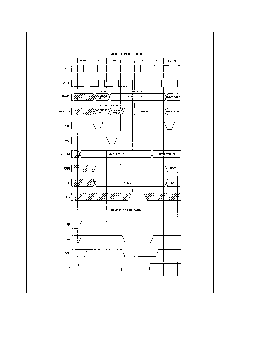
3 5 2 Translated Bus Timing
Figures 3-15 and 3-16 illustrate the CPU activity during a
Read cycle and a Write cycle in Address Translation mode
The additional T-State Tmmu is inserted between T1 and
T2 During this time the CPU places AD0 � AD15 and A16 �
A23 into the TRI-STATE
mode allowing the MMU to as-
sert the translated address and issue the physical address
strobe PAV T2 through T4 of the cycle are identical to
their counter-parts without Address Translation with the ex-
ception that the CPU Address lines A16 � A23 remain in the
TRI-STATE condition This allows the MMU to continue as-
serting the translated address on those pins
Note that in order for the NS32082 MMU to operate correct-
ly it must be set to the 32C016 mode by forcing A24 high
during reset
Figures 3-17 and 3-18 show a Read cycle and a Write cycle
as generated by the 32C016 32082 32C201 group Note
that with the CPU ADS signal going only to the MMU and
with the MMU PAV signal substituting for ADS everywhere
else Tmmu through T4 look exactly like T1 through T4 in a
non-Memory-Managed system For the connection diagram
see Appendix B
TL EE 8525 � 25
FIGURE 3-16 Write Cycle with Address Translation (CPU Action)
28

3 0 Functional Description
(Continued)
TL EE 8525 � 26
FIGURE 3-17 Memory-Managed Read Cycle
29
3 0 Functional Description
(Continued)
TL EE 8525 � 27
FIGURE 3-18 Memory-Managed Write Cycle
30
3 0 Functional Description
(Continued)
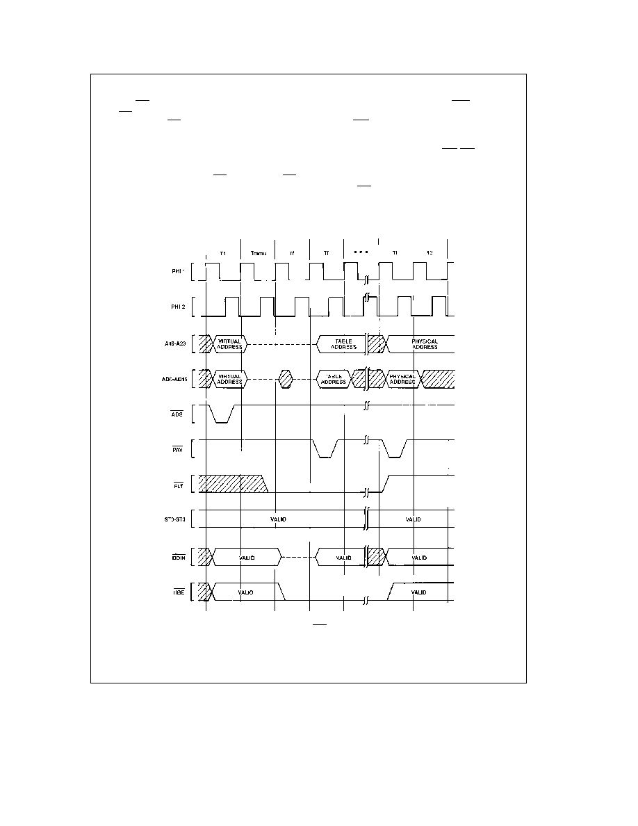
3 5 3 The FLT (Float) Pin
The FLT pin is used by the CPU for address translation
support Activating FLT during Tmmu causes the CPU to
wait longer than Tmmu for address translation and valida-
tion This feature is used occasionally by the NS32082 MMU
in order to update its internal translation Look-Aside Buffer
(TLB) from page tables in memory or to update certain
status bits within them
Figure 3-19 shows the effects of FLT Upon sampling FLT
low late in Tmmu the CPU enters idle T-States (Tf) during
which it
1)
Sets AD0 � AD15 A16 � A23 and DDIN to the TRI-
STATE condition (``floating'')
2)
Sets HBE low
3)
Suspends further internal processing of the current in-
struction This ensures that the current instruction re-
mains abortable with retry (See RST ABT description
Section 3 5 4 )
Note that the AD0 � AD15 pins may be briefly asserted dur-
ing the first idle T-State The above conditions remain in
effect until FLT again goes high See the Timing Specifica-
tions Section 4
TL EE 8525 � 28
FIGURE 3-19 FLT Timing
31

3 0 Functional Description
(Continued)
3 5 4 Aborting Bus Cycles
The RST ABT pin apart from its Reset function (Section
3 3) also serves as the means to ``abort '' or cancel a bus
cycle and the instruction if any which initiated it An Abort
request is distinguished from a Reset in that the RST ABT
pin is held active for only one clock cycle
If RST ABT is pulled low during Tmmu or Tf this signals
that the cycle must be aborted The CPU itself will enter T2
and then Ti thereby terminating the cycle Since it is the
MMU PAV signal which triggers a physical cycle the rest of
the system remains unaware that a cycle was started
The NS32082 MMU will abort a bus cycle for either of two
reasons
1)
The CPU is attempting to access a virtual address
which is not currently resident in physical memory The
reference page must be brought into physical memory
from mass storage to make it accessible to the CPU
2)
The CPU is attempting to perform an access which is
not allowed by the protection level assigned to that
page
When a bus cycle is aborted by the MMU the instruction
that caused it to occur is also aborted in such a manner that
it is guaranteed re-executable later The information that is
changed irrecoverably by such a partly-executed instruction
does not affect its re-execution
3 5 4 1 The Abort Interrupt
Upon aborting an instruction the CPU immediately performs
an interrupt through the ABT vector in the Interrupt Table
(see Section 3 8) The Return Address pushed on the Inter-
rupt Stack is the address of the aborted instruction so that
a Return from Trap (RETT) instruction will automatically re-
try it
The one exception to this sequence occurs if the aborted
bus cycle was an instruction prefetch If so it is not yet
certain that the aborted prefetched code is to be executed
Instead of causing an interrupt the CPU only aborts the bus
cycle and stops prefetching If the information in the In-
struction Queue runs out meaning that the instruction will
actually be executed the ABT interrupt will occur in effect
aborting the instruction that was being fetched
3 5 4 2 Hardware Considerations
In order to guarantee instruction retry certain rules must be
followed in applying an Abort to the CPU These rules are
followed by the NS32082 Memory Management Unit
1)
If FLT has not been applied to the CPU the Abort
pulse must occur during or before Tmmu See the Tim-
ing Specifications
Figure 4-23
2)
If FLT has been applied to the CPU the Abort pulse
must be applied before the T-State in which FLT goes
inactive The CPU will not actually respond to the Abort
command until FLT is removed See
Figure 4-24
3)
The Write half of a Read-Modify-Write operand access
may not be aborted The CPU guarantees that this will
never be necessary for Memory Management funtions
by applying a special RMW status (Status Code 1011)
during the Read half of the access When the CPU
presents RMW status that cycle must be aborted if it
would be illegal to write to any of the accessed ad-
dresses
If RST ABT is pulsed at any time other than as indicated
above it will abort either the instruction currently under exe-
cution or the next instruction and will act as a very high-pri-
ority interrupt However the program that was running at the
time is not guaranteed recoverable
3 6 BUS ACCESS CONTROL
The NS32C016 CPU has the capability of relinquishing its
access to the bus upon request from a DMA device or an-
other CPU This capability is implemented on the HOLD
(Hold Request) and HLDA (Hold Acknowledge) pins By as-
serting HOLD low an external device requests access to
the bus On receipt of HLDA from the CPU the device may
perform bus cycles as the CPU at this point has set the
AD0 � AD15 A16 � A23 ADS DDIN and HBE pins to the
TRI-STATE condition To return control of the bus to the
CPU the device sets HOLD inactive and the CPU acknowl-
edges return of the bus by setting HLDA inactive
How quickly the CPU releases the bus depends on whether
it is idle on the bus at the time the HOLD request is made
as the CPU must always complete the current bus cycle
Figure 3-20 shows the timing sequence when the CPU is
idle In this case the CPU grants the bus during the immedi-
ately following clock cycle
Figure 3-21 shows the sequence
if the CPU is using the bus at the time that the HOLD re-
quest is made If the request is made during or before the
clock cycle shown (two clock cycles before T4) the CPU
will release the bus during the clock cycle following T4 If
the request occurs closer to T4 the CPU may already have
decided to initiate another bus cycle In that case it will not
grant the bus until after the next T4 state Note that this
situation will also occur if the CPU is idle on the bus but has
initiated a bus cycle internally
In a Memory-Managed system the HLDA signal is connect-
ed in a daisy-chain through the NS32082 so that the MMU
can release the bus if it is using it
32
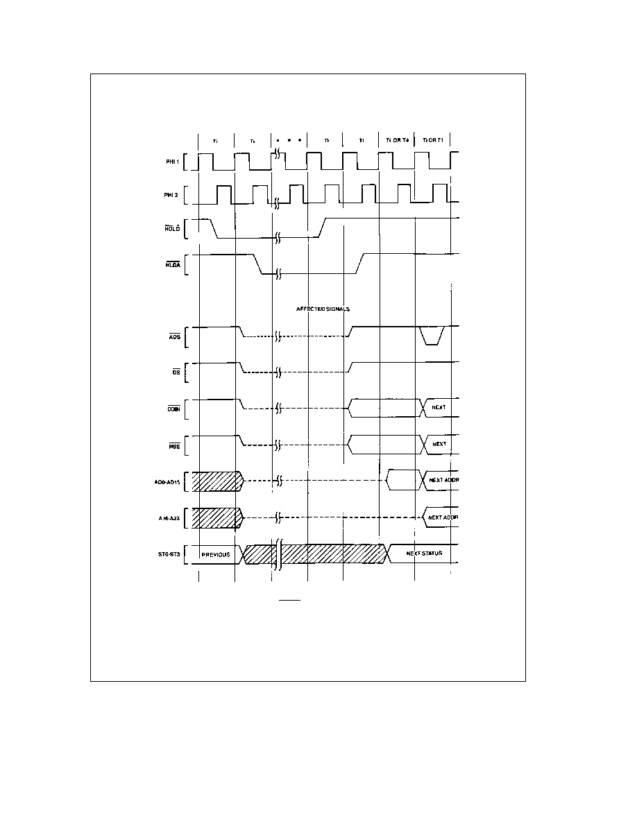
3 0 Functional Description
(Continued)
TL EE 8525 � 29
FIGURE 3-20 HOLD Timing Bus Initially Idle
33
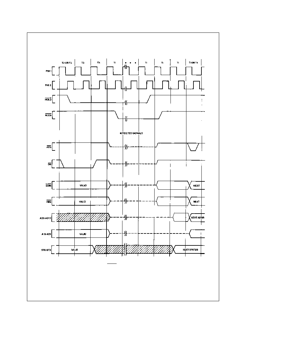
3 0 Functional Description
(Continued)
TL EE 8525 � 30
FIGURE 3-21 HOLD Timing Bus Initially Not Idle
34
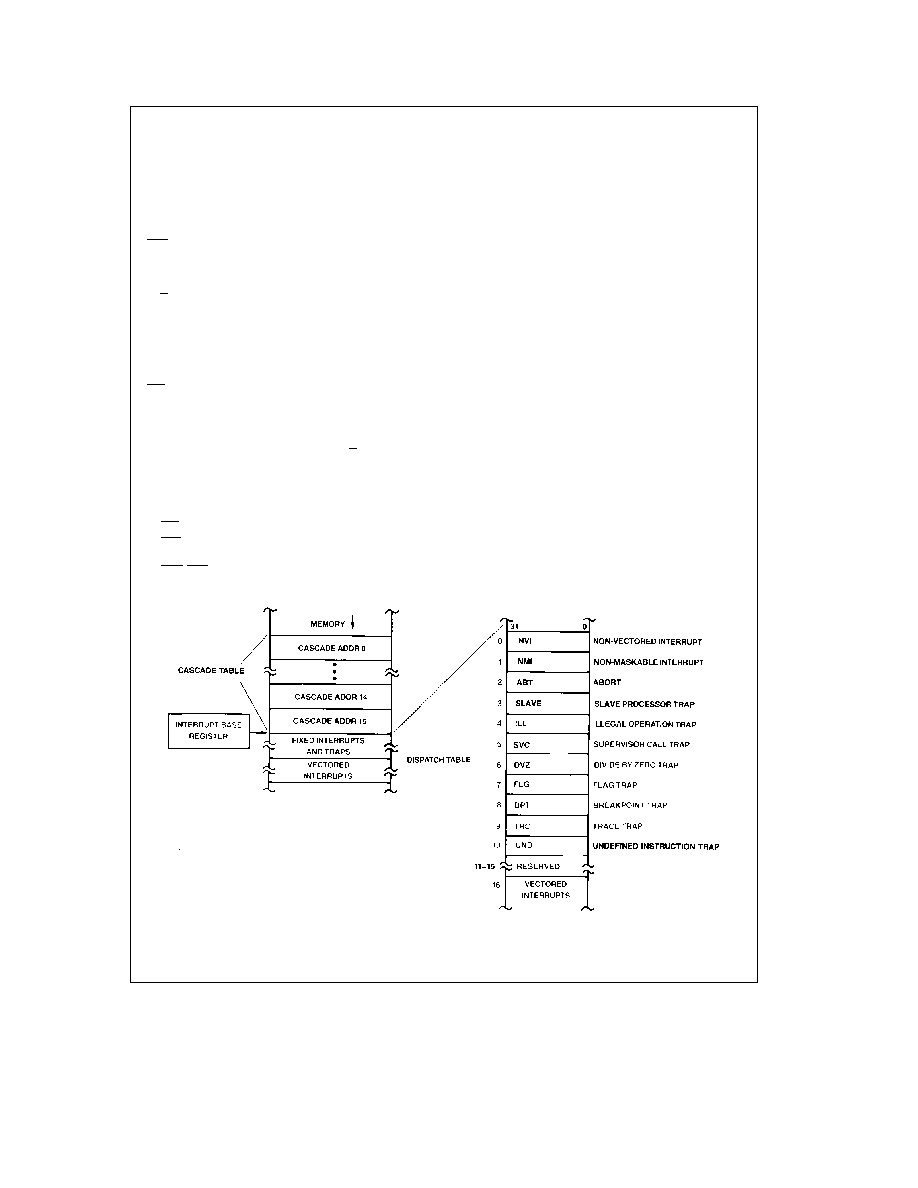
3 0 Functional Description
(Continued)
3 7 INSTRUCTION STATUS
In addition to the four bits of Bus Cycle status (ST0 � ST3)
the NS32C016 CPU also presents Instruction Status infor-
mation on three separate pins These pins differ from ST0 �
ST3 in that they are synchronous to the CPU's internal in-
struction execution section rather than to its bus interface
section
PFS (Program Flow Status) is pulsed low as each instruction
begins execution It is intended for debugging purposes and
is used that way by the NS32082 Memory Management
Unit
U S originates from the U bit of the Processor Status Regis-
ter and indicates whether the CPU is currently running in
User or Supervisor mode It is sampled by the MMU for
mapping protection and debugging purposes Although it is
not synchronous to bus cycles there are guarantees on its
validity during any given bus cycle See the Timing Specifi-
cations
Figure 4-22
ILO (Interlocked Operation) is activated during an SBITI (Set
Bit Interlocked) or CBITI (Clear Bit Interlocked) instruction
It is made available to external bus arbitration circuitry in
order to allow these instructions to implement the sema-
phore primitive operations for multi-processor communica-
tion and resource sharing As with the U S pin there are
guarantees on its validity during the operand accesses per-
formed by the instructions See the Timing Specification
Section
Figure 4-20
3 8 NS32C016 INTERRUPT STRUCTURE
INT on which maskable interrupts may be requested
NMI on which non-maskable interrupts may be request-
ed and
RST ABT which may be used to abort a bus cycle and
any associated instruction See Section 3 5 4
In addition there is a set of internally-generated ``traps''
which cause interrupt service to be performed as a result
either of exceptional conditions (e g attempted division by
zero) or of specific instructions whose purpose is to cause a
trap to occur (e g the Supervisor Call instruction)
3 8 1 General Interrupt Trap Sequence
Upon receipt of an interrupt or trap request the CPU goes
through three major steps
1)
Adjustment of Registers
Depending on the source of the interrupt or trap the
CPU may restore and or adjust the contents of the
Program Counter (PC) the Processor Status Register
(PSR) and the currently-selected Stack Pointer (SP) A
copy of the PSR is made and the PSR is then set to
reflect Supervisor Mode and selection of the Interrupt
Stack
2)
Vector Acquisition
A Vector is either obtained from the Data Bus or is
supplied by default
3)
Service Call
The Vector is used as an index into the Interrupt Dis-
patch Table whose base address is taken from the
CPU Interrupt Base (INTBASE) Register See
Figure
3-22 A 32-bit External Procedure Descriptor is read
from the table entry and an External Procedure Call is
performed using it The MOD Register (16 bits) and
Program Counter (32 bits) are pushed on the Interrupt
Stack
This process is illustrated in
Figure 3-23 from the viewpoint
of the programmer
TL EE 8525 � 31
FIGURE 3-22 Interrupt Dispatch and Cascade Tables
35
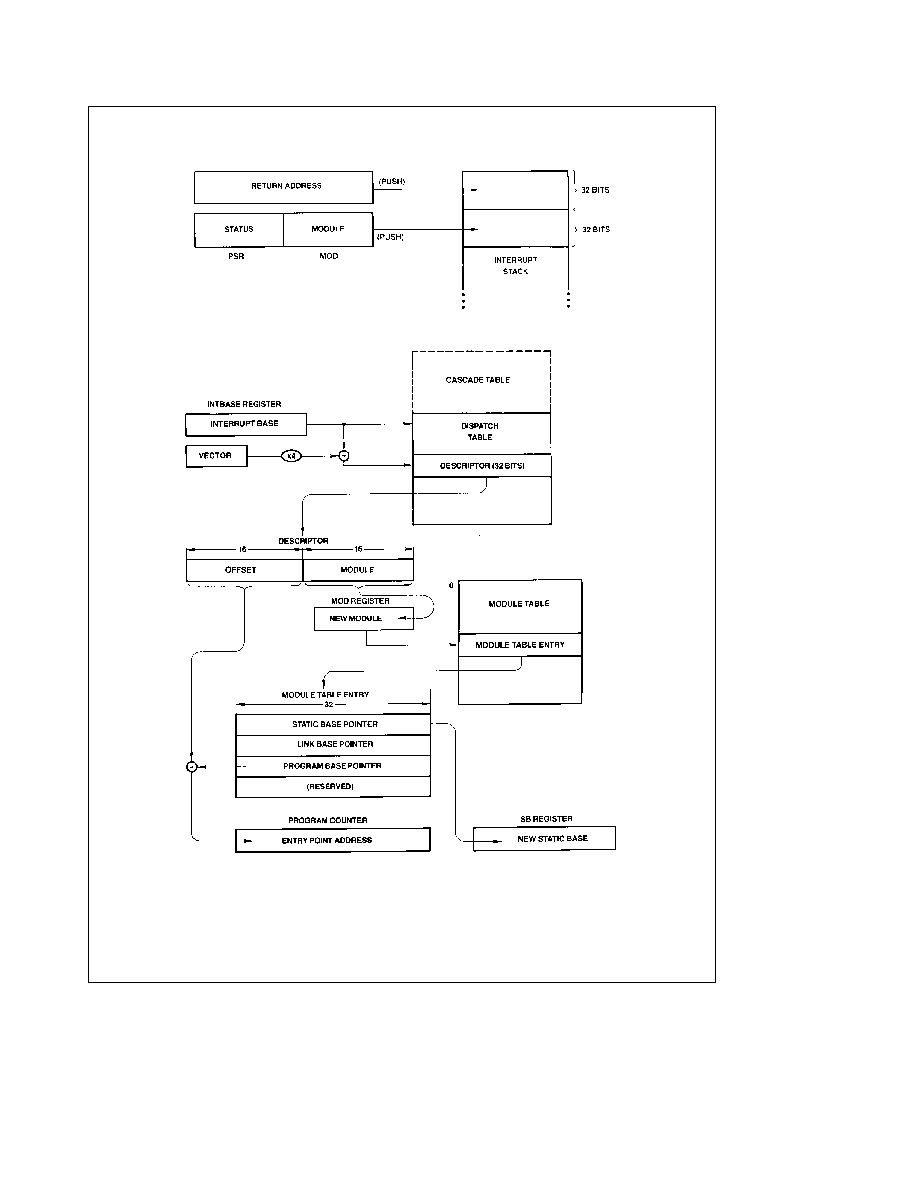
3 0 Functional Description
(Continued)
TL EE 8525 � 32
TL EE 8525 � 33
FIGURE 3-23 Interrupt Trap Service Routine Calling Sequence
36
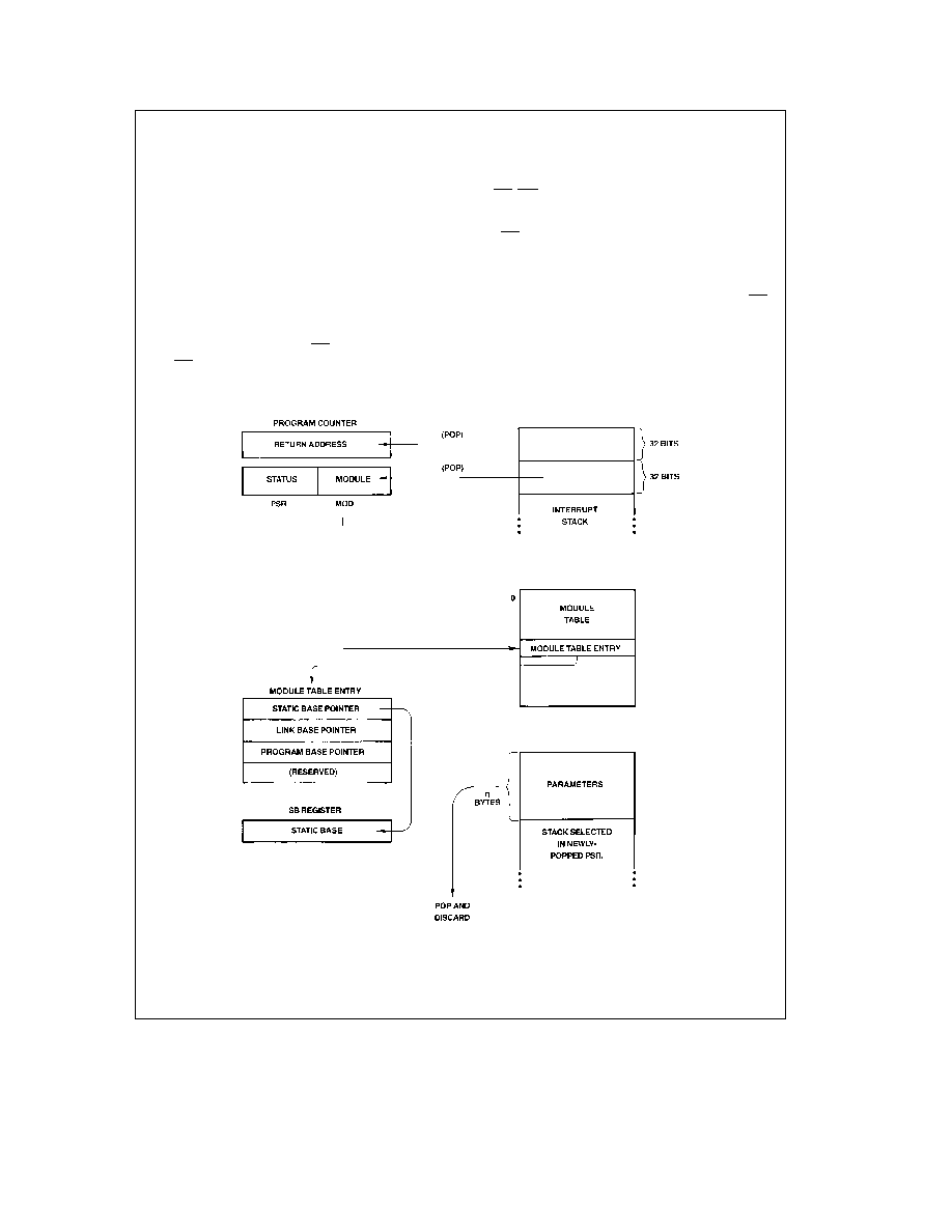
3 0 Functional Description
(Continued)
3 8 2 Interrupt Trap Return
To return control to an interrupted program one of two in-
structions is used The RETT (Return from Trap) instruction
(
Figure 3-24) restores the PSR MOD PC and SB registers
to their previous contents and since traps are often used
deliberately as a call mechanism for Supervisor Mode pro-
cedures it also discards a specified number of bytes from
the original stack as surplus parameter space RETT is used
to return from any trap or interrupt except the Maskable
Interrupt For this the RETI (Return from Interrupt) instruc-
tion is used which also informs any external Interrupt Con-
trol Units that interrupt service has completed Since inter-
rupts are generally asynchronous external events RETI
does not pop parameters See
Figure 3-25
3 8 3 Maskable Interrupts (The INT Pin)
The INT pin is a level-sensitive input A continuous low level
is allowed for generating multiple interrupt requests The
input is maskable and is therefore enabled to generate in-
terrupt requests only while the Processor Status Register I
bit is set The I bit is automatically cleared during service of
an INT NMI or Abort request and is restored to its original
setting upon return from the interrupt service routine via the
RETT or RETI instruction
The INT pin may be configured via the SETCFG instruction
as either Non-Vectored (CFG Register bit I
e
0) or Vectored
(bit I
e
1)
3 8 3 1 Non-Vectored Mode
In the Non-Vectored mode an interrupt request on the INT
pin will cause an Interrupt Acknowledge bus cycle but the
CPU will ignore any value read from the bus and use instead
a default vector of zero This mode is useful for small sys-
tems in which hardware interrupt prioritization is unneces-
sary
TL EE 8525 � 34
FIGURE 3-24 Return from Trap (RETT n) Instruction Flow
37
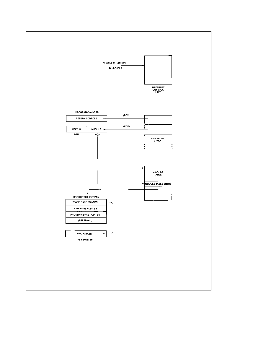
3 0 Functional Description
(Continued)
TL EE 8525 � 35
FIGURE 3-25 Return from Interrupt (RET I) Instruction Flow
38

3 0 Functional Description
(Continued)
3 8 3 2 Vectored Mode Non-Cascaded Case
In the Vectored mode the CPU uses an Interrupt Control
Unit (ICU) to prioritize up to 16 interrupt requests Upon re-
ceipt of an interrupt request on the INT pin the CPU per-
forms an ``Interrupt Acknowledge Master'' bus cycle (Sec-
tion 3 4 2) reading a vector value from the low-order byte of
the Data Bus This vector is then used as an index into the
Dispatch Table in order to find the External Procedure De-
scriptor for the proper interrupt service procedure The serv-
ice procedure eventually returns via the Return from Inter-
rupt (RETI) instruction which performs an End of Interrupt
bus cycle informing the ICU that it may re-prioritize any in-
terrupt requests still pending The ICU provides the vector
number again which the CPU uses to determine whether it
needs also to inform a Cascaded ICU (see below)
In a system with only one ICU (16 levels of interrupt) the
vectors provided must be in the range of 0 through 127 that
is they must be positive numbers in eight bits By providing
a negative vector number an ICU flags the interrupt source
as being a Cascaded ICU (see below)
3 8 3 3 Vectored Mode Cascaded Case
In order to allow up to 256 levels of interrupt provision is
made both in the CPU and in the NS32202 Interrupt Control
Unit (ICU) to transparently support cascading
Figure 3-27
shows a typical cascaded configuration Note that the Inter-
rupt output from a Cascaded ICU goes to an Interrupt Re-
quest input of the Master ICU which is the only ICU which
drives the CPU INT pin
In a system which uses cascading two tasks must be per-
formed upon initialization
1)
For each Cascaded ICU in the system the Master ICU
must be informed of the line number (0 to 15) on which
it receives the cascaded requests
2)
A Cascade Table must be established in memory The
Cascade Table is located in a NEGATIVE direction
from the location indicated by the CPU Interrupt Base
(INTBASE) Register Its entries are 32-bit addresses
pointing to the Vector Registers of each of up to 16
Cascaded ICUs
Figure 3-22 illustrates the position of the Cascade Table To
find the Cascade Table entry for a Cascaded ICU take its
Master ICU line number (0 to 15) and subtract 16 from it
giving an index in the range
b
16 to
b
1 Multiply this value
by 4 and add the resulting negative number to the contents
of the INTBASE Register The 32-bit entry at this address
must be set to the address of the Hardware Vector Register
of the Cascaded ICU This is referred to as the ``Cascade
Address ''
Upon receipt of an interrupt request from a Cascaded ICU
the Master ICU interrupts the CPU and provides the nega-
tive Cascade Table index instead of a (positive) vector num-
ber The CPU seeing the negative value uses it as an index
into the Cascade Table and reads the Cascade Address
from the referenced entry Applying this address the CPU
performs an ``Interrupt Acknowledge Cascaded'' bus cycle
(Section 3 4 2) reading the final vector value This vector is
interpreted by the CPU as an unsigned byte and can there-
fore be in the range of 0 through 255
In returning from a Cascaded interrupt the service proce-
dure executes the Return from Interrupt (RETI) instruction
as it would for any Maskable Interrupt The CPU performs
an ``End of Interrupt Master'' bus cycle (Section 3 4 2)
whereupon the Master ICU again provides the negative
Cascaded Table index The CPU seeing a negative value
uses it to find the corresponding Cascade Address from the
Cascade Table Applying this address it performs an ``End
of Interrupt Cascaded'' bus cycle (Section 3 4 2) informing
the Cascaded ICU of the completion of the service routine
The byte read from the Cascaded ICU is discarded
Note
If an interrupt must be masked off the CPU can do so by setting the
corresponding bit in the Interrupt Mask Register of the Interrupt Con-
troller However if an interrupt is set pending during the CPU instruc-
tion that masks off that interrupt the CPU may still perform an inter-
rupt acknowledge cycle following that instruction since it might have
sampled the INT line before the ICU deasserted it This could cause
the ICU to provide an invalid vector To avoid this problem the above
operation should be performed with the CPU interrupt disabled
TL EE 8525 � 36
FIGURE 3-26 Interrupt Control Unit Connections (16 Levels)
39
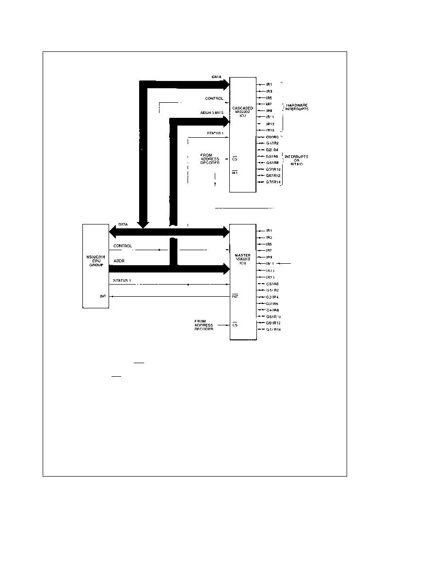
3 0 Functional Description
(Continued)
TL EE 8525 � 37
FIGURE 3-27 Cascaded Interrupt Control Unit Connections
3 8 4 Non-Maskable Interrupt (The NMI Pin)
The Non-Maskable Interrupt is triggered whenever a falling
edge is detected on the NMI pin The CPU performs an
``Interrupt Acknowledge Master'' bus cycle (Section 3 4 2)
when processing of this interrupt actually begins The Inter-
rupt Acknowledge cycle differs from that provided for Mask-
able Interrupts in that the address presented is FFFF00
16
The vector value used for the Non-Maskable Interrupt is
taken as 1 regardless of the value read from the bus
The service procedure returns from the Non-Maskable In-
terrupt using the Return from Trap (RETT) instruction No
special bus cycles occur on return
For the full sequence of events in processing the Non-
Maskable Interrupt see Section 3 8 7 1
3 8 5 Traps
A trap is an internally-generated interrupt request caused as
a direct and immediate result of the execution of an instruc-
tion The Return Address pushed by any trap except Trap
(TRC) below is the address of the first byte of the instruction
during which the trap occurred Traps do not disable inter-
rupts as they are not associated with external events Traps
recognized by NS32C016 CPU are
Trap (SLAVE)
An exceptional condition was detected by
the Floating Point Unit or another Slave Processor during
the execution of a Slave Instruction This trap is requested
via the Status Word returned as part of the Slave Processor
Protocol (Section 3 9 1)
40

3 0 Functional Description
(Continued)
Trap (ILL)
Illegal operation A privileged operation was at-
tempted while the CPU was in User Mode (PSR bit U
e
1)
Trap (SVC)
The Supervisor Call (SVC) instruction was exe-
cuted
Trap (DVZ)
An attempt was made to divide an integer by
zero (The Slave trap is used for Floating Point division by
zero )
Trap (FLG)
The FLAG instruction detected a ``1'' in the
CPU PSR F bit
Trap (BPT)
The Breakpoint (BPT) instruction was execut-
ed
Trap (TRC)
The instruction just completed is being traced
See below
Trap (UND)
An undefined opcode was encountered by the
CPU
A special case is the Trace Trap (TRC) which is enabled by
setting the T bit in the Processor Status Register (PSR) At
the beginning of each instruction the T bit is copied into the
PSR P (Trace ``Pending'') bit If the P bit is set at the end of
an instruction then the Trace Trap is activated If any other
trap or interrupt request is made during a traced instruction
its entire service procedure is allowed to complete before
the Trace Trap occurs Each interrupt and trap sequence
handles the P bit for proper tracing guaranteeing one and
only one Trace Trap per instruction and guaranteeing that
the Return Address pushed during a Trace Trap is always
the address of the next instruction to be traced
3 8 6 Prioritization
The NS32C016 CPU internally prioritizes simultaneous inter-
rupt and trap requests as follows
1) Traps other than Trace
(Highest priority)
2) Abort
3) Non-Maskable Interrupt
4) Maskable Interrupts
5) Trace Trap
(Lowest priority)
3 8 7 Interrupt Trap Sequences Detail Flow
For purposes of the following detailed discussion of inter-
rupt and trap service sequences a single sequence called
``Service'' is defined in
Figure 3-28 Upon detecting any in-
terrupt request or trap condition the CPU first performs a
sequence dependent upon the type of interrupt or trap This
sequence will include pushing the Processor Status Regis-
ter and establishing a Vector and a Return Address The
CPU then performs the Service sequence
For the sequenced followed in processing either Maskable
or Non-Maskable Interrupts (on the INT or NMI pins respec-
tively) see Section 3 8 7 1 For Abort interrupts see Section
3 8 7 4 For the Trace Trap see Section 3 8 7 3 and for all
other traps see Section 3 8 7 2
3 8 7 1 Maskable Non-Maskable Interrupt Sequence
This sequence is performed by the CPU when the NMI pin
receives a falling edge or the INT pin becomes active with
the PSR I bit set The interrupt sequence begins either at
the next instruction boundary or in the case of the String
instructions at the next interruptible point during its execu-
tion
1
If a String instruction was interrupted and not yet com-
pleted
a
Clear the Processor Status Register P bit
b
Set ``Return Address'' to the address of the first
byte of the interrupted instruction
Otherwise set ``Return Address'' to the address of the
next instruction
2
Copy the Processor Status Register (PSR) into a tem-
porary register then clear PSR bits S U T P and I
3
If the interrupt is Non-Maskable
a
Read a byte from address FFFF00
16
applying
Status Code 0100 (Interrupt Acknowledge Mas-
ter Section 3 4 2) Discard the byte read
b
Set ``Vector'' to 1
c
Go to Step 8
4
If the interrupt is Non-Vectored
a
Read a byte from address FFFF00
16
applying
Status Code 0100 (Interrupt Acknowledge Mas-
ter Section 3 4 2) Discard the byte read
b
Set ``Vector'' to 0
c
Go to Step 8
5
Here the interrupt is Vectored Read ``Byte'' from ad-
dress FFFE00
16
applying Status Code 0100 (Interrupt
Acknowledge Master Section 3 4 2)
6
If ``Byte''
t
0 then set ``Vector'' to ``Byte'' and go to
Step 8
7
If ``Byte'' is in the range
b
16 through
b
1 then the
interrupt source is Cascaded (More negative values
are reserved for future use ) Perform the following
a
Read the 32-bit Cascade Address from memory
The address is calculated as INTBASE
a
4 Byte
b
Read ``Vector '' applying the Cascade Address
just read and Status Code 0101 (Interrupt Ac-
knowledge Cascaded Section 3 4 2)
8
Push the PSR copy (from Step 2) onto the Interrupt
Stack as a 16-bit value
9
Perform Service (Vector Return Address)
Figure 3-28
Service (Vector Return Address)
1)
Read the 32-bit External Procedure Descriptor from the Interrupt Dis-
patch Table address is Vector 4
a
INTBASE Register contents
2)
Move the Module field of the Descriptor into the MOD Register
3)
Read the new Static Base pointer from the memory address contained
in MOD placing it into the SB Register
4)
Read the Program Base pointer from memory address MOD
a
8 and
add to it the Offset field from the Descriptor placing the result in the
Program Counter
5)
Flush Queue Non-sequentially fetch first instruction of Interrupt Rou-
tine
6)
Push MOD Register onto the Interrupt Stack as a 16-bit value (The
PSR has already been pushed as a 16-bit value )
7)
Push the Return Address onto the Interrupt Stack as a 32-bit quantity
FIGURE 3-28 Service Sequence
Invoked during all interrupt trap sequences
41

3 0 Functional Description
(Continued)
3 8 7 2 Trap Sequence Traps Other Than Trace
1)
Restore the currently selected Stack Pointer and the
Processor Status Register to their original values at the
start of the trapped instruction
2)
Set ``Vector'' to the value corresponding to the trap
type
SLAVE
Vector
e
3
ILL
Vector
e
4
SVC
Vector
e
5
DVZ
Vector
e
6
FLG
Vector
e
7
BPT
Vector
e
8
UND
Vector
e
10
3)
Copy the Processor Status Register (PSR) into a tem-
porary register then clear PSR bits S U P and T
4)
Push the PSR copy onto the Interrupt Stack as a 16-bit
value
5)
Set ``Return Address'' to the address of the first byte of
the trapped instruction
6)
Perform Service (Vector Return Address)
Figure 3-28
3 8 7 3 Trace Trap Sequence
1)
In the Processor Status Register (PSR) clear the P bit
2)
Copy the PSR into a temporary register then clear
PSR bits S U and T
3)
Push the PSR copy onto the Interrupt Stack as a 16-bit
value
4)
Set ``Vector'' to 9
5)
Set ``Return Address'' to the address of the next in-
struction
6)
Perform Service (Vector Return Address)
Figure 3-28
3 8 7 4 Abort Sequence
1)
Restore the currently selected Stack Pointer to its origi-
nal contents at the beginning of the aborted instruction
2)
Clear the PSR P bit
3)
Copy the PSR into a temporary register then clear
PSR bits S U T and I
4)
Push the PSR copy onto the Interrupt Stack as a 16-bit
value
5)
Set ``Vector'' to 2
6)
Set ``Return Address'' to the address of the first byte of
the aborted instruction
7)
Perform Service (Vector Return Address)
Figure 3-28
3 9 SLAVE PROCESSOR INSTRUCTIONS
The NS32C016 CPU recognizes three groups of instructions
as being executable by external Slave Processors
Floating Point Instruction Set
Memory Management Instruction Set
Custom Instruction Set
Each Slave Instruction Set is validated by a bit in the Config-
uration Register (Section 2 1 3) Any Slave Instruction which
does not have its corresponding Configuration Register bit
set will trap as undefined without any Slave Processor com-
munication attempted by the CPU This allows software sim-
ulation of a non-existent Slave Processor
3 9 1 Slave Processor Protocol
Slave Processor instructions have a three-byte Basic In-
struction field consisting of an ID Byte followed by an Oper-
ation Word The ID Byte has three functions
1)
It identifies the instruction as being a Slave Processor
instruction
2)
It specifies which Slave Processor will execute it
3)
It determines the format of the following Operation
Word of the instruction
Upon receiving a Slave Processor instruction the CPU initi-
ates the sequence outlined in
Figure 3-29 While applying
Status Code 1111 (Broadcast ID Section 3 4 2) the CPU
transfers the ID Byte on the least-significant half of the Data
Bus (AD0 � AD7) All Slave Processors input this byte and
decode it The Slave Processor selected by the ID Byte is
activated and from this point the CPU is communicating
only with it If any other slave protocol was in progress (e g
an aborted Slave instruction) this transfer cancels it
The CPU next sends the Operation Word while applying
Status Code 1101 (Transfer Slave Operand Section 3 4 2)
Upon receiving it the Slave Processor decodes it and at
this point both the CPU and the Slave Processor are aware
of the number of operands to be transferred and their sizes
The Operation Word is swapped on the Data Bus that is
bits 0 � 7 appear on pins AD8 � AD15 and bits 8 � 15 appear
on pins AD0 � AD7
Using the Addressing Mode fields within the Operation
Word the CPU starts fetching operands and issuing them to
the Slave Processor To do so it references any Addressing
Mode extensions which may be appended to the Slave
Processor instruction Since the CPU is solely responsible
for memory accesses these extensions are not sent to the
Slave Processor The Status Code applied is 1101 (Transfer
Slave Processor Operand Section 3 4 2)
Status Combinations
Send ID (ID) Code 1111
Xfer Operand (OP) Code 1101
Read Status (ST) Code 1110
Step Status
Action
1
ID
CPU Send ID Byte
2
OP
CPU Sends Operation Word
3
OP
CPU Sends Required Operands
4
Slave Starts Execution CPU Pre-Fetches
5
Slave Pulses SPC Low
6
ST
CPU Reads Status Word (Trap Alter Flags )
7
OP
CPU Reads Results (If Any)
FIGURE 3-29 Slave Processor Protocol
42

3 0 Functional Description
(Continued)
After the CPU has issued the last operand the Slave Proc-
essor starts the actual execution of the instruction Upon
completion it will signal the CPU by pulsing SPC low To
allow for this and for the Address Translation strap func-
tion AT SPC is normally held high only by an internal pull-
up device of approximately 5 kX
While the Slave Processor is executing the instruction the
CPU is free to prefetch instructions into its queue If it fills
the queue before the Slave Processor finishes the CPU will
wait applying Status Code 0011 (Waiting for Slave Section
3 4 2)
Upon receiving the pulse on SPC the CPU uses SPC to
read a Status Word from the Slave Processor applying
Status Code 1110 (Read Slave Status Section 3 4 2) This
word has the format shown in
Figure 3-30 If the Q bit
(``Quit'' Bit 0) is set this indicates that an error was detect-
ed by the Slave Processor The CPU will not continue the
protocol but will immediately trap through the Slave vector
in the Interrupt Table Certain Slave Processor instructions
cause CPU PSR bits to be loaded from the Status Word
The last step in the protocol is for the CPU to read a result
if any and transfer it to the destination The Read cycles
from the Slave Processor are performed by the CPU while
applying Status Code 1101 (Transfer Slave Operand Sec-
tion 3 4 2)
An exception to the protocol above is the LMR (Load Mem-
ory Management Register) instruction and a corresponding
Custom Slave instruction (LCR Load Custom Register) In
executing these instructions the protocol ends after the
CPU has issued the last operand The CPU does not wait for
an acknowledgement from the Slave Processor and it does
not read status
3 9 2 Floating Point Instructions
Table 3-4 gives the protocols followed for each Floating
Point instruction The instructions are referenced by their
mnemonics For the bit encodings of each instruction see
Appendix A
The Operand class columns give the Access Class for each
general operand defining how the addressing modes are
interpreted (see Series 32000 Instruction Set Reference
Manual)
The Operand Issued columns show the sizes of the oper-
ands issued to the Floating Point Unit by the CPU ``D'' indi-
cates a 32-bit Double Word ``i'' indicates that the instruction
specifies an integer size for the operand (B
e
Byte
W
e
Word D
e
Double Word) ``f'' indicates that the instruc-
tion specifies a Floating Point size for the operand (F
e
32-
bit Standard Floating L
e
64-bit Long Floating)
The Returned Value Type and Destination column gives the
size of any returned value and where the CPU places it The
PSR Bits Affected column indicates which PSR bits if any
are updated from the Slave Processor Status Word (
Figure
3-30)
TABLE 3-4 Floating Point Instruction Protocols
Operand 1
Operand 2
Operand 1
Operand 2
Returned Value
PSR Bits
Mnemonic
Class
Class
Issued
Issued
Type and Dest
Affected
ADDf
read f
rmw f
f
f
f to Op 2
none
SUBf
read f
rmw f
f
f
f to Op 2
none
MULf
read f
rmw f
f
f
f to Op 2
none
DIVf
read f
rmw f
f
f
f to Op 2
none
MOVf
read f
write f
f
N A
f to Op 2
none
ABSf
read f
write f
f
N A
f to Op 2
none
NEGf
read f
write f
f
N A
f to Op 2
none
CMPf
read f
read f
f
f
N A
N Z L
FLOORfi
read f
write i
f
N A
i to Op 2
none
TRUNCfi
read f
write i
f
N A
i to Op 2
none
ROUNDfi
read f
write i
f
N A
i to Op 2
none
MOVFL
read F
write L
F
N A
L to Op 2
none
MOVLF
read L
write F
L
N A
F to Op 2
none
MOVif
read i
write f
i
N A
f to Op 2
none
LFSR
read D
N A
D
N A
N A
none
SFSR
N A
write D
N A
N A
D to Op 2
none
Notes
D
e
Double Word
i
e
integer size (B W D) specified in mnemonic
f
e
Floating Point type (F L) specified in mnemonic
N A
e
Not Applicable to this instruction
43

3 0 Functional Description
(Continued)
TL EE 8525 � 38
FIGURE 3-30 Slave Processor Status Word Format
Any operand indicated as being of type ``f'' will not cause a
transfer if the Register addressing mode is specified This is
because the Floating Point Registers are physically on the
Floating Point Unit and are therefore available without CPU
assistance
3 9 3 Memory Management Instructions
Table 3-5 gives the protocols for Memory Management in-
structions Encodings for these instructions may be found in
Appendix A
In executing the RDVAL and WRVAL instructions the CPU
calculates and issues the 32-bit Effective Address of the
single operand The CPU then performs a single-byte Read
cycle from that address allowing the MMU to safely abort
the instruction if the necessary information is not currently in
physical memory Upon seeing the memory cycle complete
the MMU continues the protocol and returns the validation
result in the F bit of the Slave Status Word
The size of a Memory Management operand is always a 32-
bit Double Word For further details of the Memory Manage-
ment Instruction set see the Series 32000 Instruction Set
Reference Manual and the NS32082 MMU Data Sheet
TABLE 3-5 Memory Management Instruction Protocols
Operand 1
Operand 2
Operand 1
Operand 2
Returned Value
PSR Bits
Mnemonic
Class
Class
Issued
Issued
Type and Dest
Affected
RDVAL
addr
N A
D
N A
N A
F
WRVAL
addr
N A
D
N A
N A
F
LMR
read D
N A
D
N A
N A
none
SMR
write D
N A
N A
N A
D to Op 1
none
Note
In the RDVAL and WRVAL instructions the CPU issues the address as a Double Word and performs a single-byte Read cycle from that memory address For
details see the Series 32000 Instruction Set Reference Manual and the NS32082 Memory Management Unit Data Sheet
D
e
Double Word
e
Privileged Instruction will trap if CPU is in User Mode
N A
e
Not Applicable to this instruction
44

3 0 Functional Description
(Continued)
3 9 4 Custom Slave Instructions
Provided in the NS32C016 is the capability of communicat-
ing with a user-defined ``Custom'' Slave Processor The in-
struction set provided for a Custom Slave Processor defines
the instruction formats the operand classes and the com-
munication protocol Left to the user are the interpretations
of the Op Code fields the programming model of the Cus-
tom Slave and the actual types of data transferred The pro-
tocol specifies only the size of an operand not its data type
Table 3-6 lists the relevant information for the Custom Slave
instruction set The designation ``c'' is used to represent an
operand which can be a 32-bit (``D'') or 64-bit (``Q'') quantity
in any format the size is determined by the suffix on the
mnemonic Similarly an ``i'' indicates an integer size (Byte
Word Double Word) selected by the corresponding mne-
monic suffix
Any operand indicated as being of type `c' will not cause a
transfer if the register addressing mode is specified It is
assumed in this case that the slave processor is already
holding the operand internally
For the instruction encodings see Appendix A
TABLE 3-6 Custom Slave Instruction Protocols
Operand 1
Operand 2
Operand 1
Operand 2
Returned Value
PSR Bits
Mnemonic
Class
Class
Issued
Issued
Type and Dest
Affected
CCAL0c
read c
rmw c
c
c
c to Op 2
none
CCAL1c
read c
rmw c
c
c
c to Op 2
none
CCAL2c
read c
rmw c
c
c
c to Op 2
none
CCAL3c
read c
rmw c
c
c
c to Op 2
none
CMOV0c
read c
write c
c
N A
c to Op 2
none
CMOV1c
read c
write c
c
N A
c to Op 2
none
CMOV2c
read c
write c
c
N A
c to Op 2
none
CMOV3c
read c
write c
c
N A
c to Op 2
none
CCMP0c
read c
read c
c
c
N A
N Z L
CCMP1c
read c
read c
c
c
N A
N Z L
CCV0ci
read c
write i
c
N A
i to Op 2
none
CCV1ci
read c
write i
c
N A
i to Op 2
none
CCV2ci
read c
write i
c
N A
i to Op 2
none
CCV3ic
readi
write c
i
N A
c to Op 2
none
CCV4DQ
read D
write Q
D
N A
Q to Op 2
none
CCV5QD
read Q
write D
Q
N A
D to Op 2
none
LCSR
read D
N A
D
N A
N A
none
SCSR
N A
write D
N A
N A
D to Op 2
none
CATST0
addr
N A
D
N A
N A
F
CATST1
addr
N A
D
N A
N A
F
LCR
read D
N A
D
N A
N A
none
SCR
write D
N A
N A
N A
D to Op 1
none
Notes
D
e
Double Word
i
e
integer size (B W D) specified in mnemonic
c
e
Custom size (D 32 bits or Q 64 bits) specified in mnemonic
e
Privileged instruction will trap if CPU is in User Mode
N A
e
Not Applicable to this instruction
45

4 0 Device Specifications
4 1 NS32C016 PIN DESCRIPTIONS
The following is a brief description of all NS32C016 pins
The descriptions reference portions of the Functional De-
scription Section 3
4 1 1 Supplies
Logic Power (V
CCL
)
a
5V positive supply for on-chip logic
Section 3 1
Buffer Power (V
CCB
)
a
5V positive supply for on-chip out-
put buffers Section 3 1
Logic Ground (GNDL)
Ground reference for on-chip logic
Section 3 1
Buffer Ground (GNDB)
Ground reference for on-chip driv-
ers connected to output pins Section 3 1
4 1 2 Input Signals
Clocks (PHI1 PHI2)
Two-phase clocking signals Section
3 2
Ready (RDY)
Active high While RDY is inactive the CPU
extends the current bus cycle to provide for a slower memo-
ry or peripheral reference Upon detecting RDY active the
CPU terminates the bus cycle Section 3 4 1
Hold Request (HOLD)
Active low Causes the CPU to re-
lease the bus for DMA or multiprocessing purposes Section
3 6
Note
If the HOLD signal is generated asynchronously its set up and hold
times may be violated In this case it is recommended to synchronize
it with CTTL to minimize the possibility of metastable states
The CPU provides only one synchronization stage to minimize the
HLDA latency This is to avoid speed degradations in cases of heavy
HOLD activity (i e DMA controller cycles interleaved with CPU cy-
cles)
Interrupt (INT)
Active low Maskable Interrupt request
Section 3 8
Non-Maskable Interrupt (NMI)
Active low Non-Maskable
Interrupt request Section 3 8
Reset Abort (RST ABT)
Active low If held active for one
clock cycle and released this pin causes an Abort Com-
mand Section 3 5 4 If held longer it initiates a Reset Sec-
tion 3 3
4 1 3 Output Signals
Address Bits 16 � 23 (A16 � A23)
These are the most sig-
nificant 8 bits of the memory address bus Section 3 4
Address Strobe (ADS)
Active low Controls address latch-
es indicates start of a bus cycle Section 3 4
Data Direction In (DDIN)
Active low Status signal indicat-
ing direction of data transfer during a bus cycle Section 3 4
High Byte Enable (HBE)
Active low Status signal enabling
transfer on the most significant byte of the Data Bus Sec-
tion 3 4 Section 3 4 3
Note
In the current NS32C016 the HBE signal is forced low by the CPU
when FLT is asserted by the MMU However in future revisions of the
CPU HBE will no longer be affected by FLT Therefore in a memory
managed system an external `AND' gate is required This is shown in
Figure B-1 in Appendix B
Status (ST0 � ST3)
Active high Bus cycle status code ST0
least significant Section 3 4 2 Encodings are
0000
Idle CPU Inactive on Bus
0001
Idle WAIT Instruction
0010
(Reserved)
0011
Idle Waiting for Slave
0100
Interrupt Acknowledge Master
0101
Interrupt Acknowledge Cascaded
0110
End of Interrupt Master
0111
End of Interrupt Cascaded
1000
Sequential Instruction Fetch
1001
Non-Sequential Instruction Fetch
1010
Data Transfer
1011
Read Read-Modify-Write Operand
1100
Read for Effective Address
1101
Transfer Slave Operand
1110
Read Slave Status Word
1111
Broadcast Slave ID
Hold Acknowledge (HLDA)
Active low Applied by the
CPU in response to HOLD input indicating that the bus has
been released for DMA or multiprocessing purposes Sec-
tion 3 6
User Supervisor (U S)
User or Supervisor Mode status
Section 3 7 High state indicates User Mode low indicates
Supervisor Mode Section 3 7
Interlocked Operation (ILO)
Active low Indicates that an
interlocked instruction is being executed Section 3 7
Program Flow Status (PFS)
Active Low Pulse indicates
beginning of an instruction execution Section 3 7
4 1 4 Input-Output Signals
Address Data 0 � 15 (AD0 � AD15)
Multiplexed Address
Data information Bit 0 is the least significant bit of each
Section 3 4
Address
Translation Slave
Processor
Control
(AT SPC)
Active low Used by the CPU as the data strobe
output for Slave Processor transfers used by Slave Proces-
sors to acknowledge completion of a slave instruction Sec-
tion 3 4 6 Section 3 9 Sampled on the rising edge of Reset
as Address Translation Strap Section 3 5 1
In non-memory-managed systems this pin should be pulled
up to V
CC
through a 10 kX resistor
Data Strobe Float (DS FLT)
Active low Data Strobe out-
put Section 3 4 or Float Command input Section 3 5 3 Pin
function is selected on AT SPC pin Section 3 5 1
46
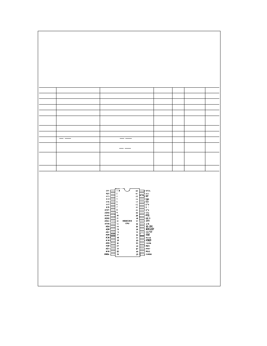
4 0 Device Specifications
(Continued)
4 2 ABSOLUTE MAXIMUM RATINGS
If Military Aerospace specified devices are required
please contact the National Semiconductor Sales
Office Distributors for availability and specifications
Temperature Under Bias
0 C to
a
70 C
Storage Temperature
b
65 C to
a
150 C
All Input or Output Voltages with
Respect to GND
b
0 5V to
a
7V
Power Dissipation
1 5 Watt
Note
Absolute maximum ratings indicate limits beyond
which permanent damage may occur Continuous operation
at these limits is not intended operation should be limited to
those conditions specified under Electrical Characteristics
4 3 ELECTRICAL CHARACTERISTICS
T
A
e b
40 C to
a
85 C V
CC
e
5V
g
10% GND
e
0V
Symbol
Parameter
Conditions
Min
Typ
Max
Units
V
IH
High Level Input Voltage
2 0
V
CC
a
0 5
V
V
IL
Low Level Input Voltage
b
0 5
0 8
V
V
CH
High Level Clock Voltage
PHI1 PHI2 pins only
0 90 V
CC
V
CC
a
0 5
V
V
CL
Low Level Clock Voltage
PHI1 PHI2 pins only
b
0 5
0 10 V
CC
V
V
CRT
Clock Input
PHI1 PHI2 pins only
b
0 5
0 6
V
Ringing Tolerance
V
OH
High Level Output Voltage
I
OH
e b
400 mA
0 90 V
CC
V
V
OL
Low Level Output Voltage
I
OL
e
2 mA
0 10 V
CC
V
I
ILS
AT SPC Input Current (low)
V
IN
e
0 4V AT SPC in input mode
0 05
1 0
mA
I
I
Input Load Current
0
s
V
IN
s
V
CC
All inputs except
b
20
20
m
A
PHI1 PHI2 AT SPC
I
L
Leakage Current Output
and IO Pins in TRI-STATE
0 4
s
V
IN
s
V
CC
b
20
20
m
A
Input Mode
I
CC
Active Supply Current
I
OUT
e
0 T
A
e
25 C
70
100
mA
Connection Diagram
Dual-In-Line Package
TL EE 8525 � 2
Top View
FIGURE 4-1
Order Number NS32C016D-10 NS32C016D-15
NS32C016N-10 or NS32C016N-15
See NS Package Number D48A or N48A
47
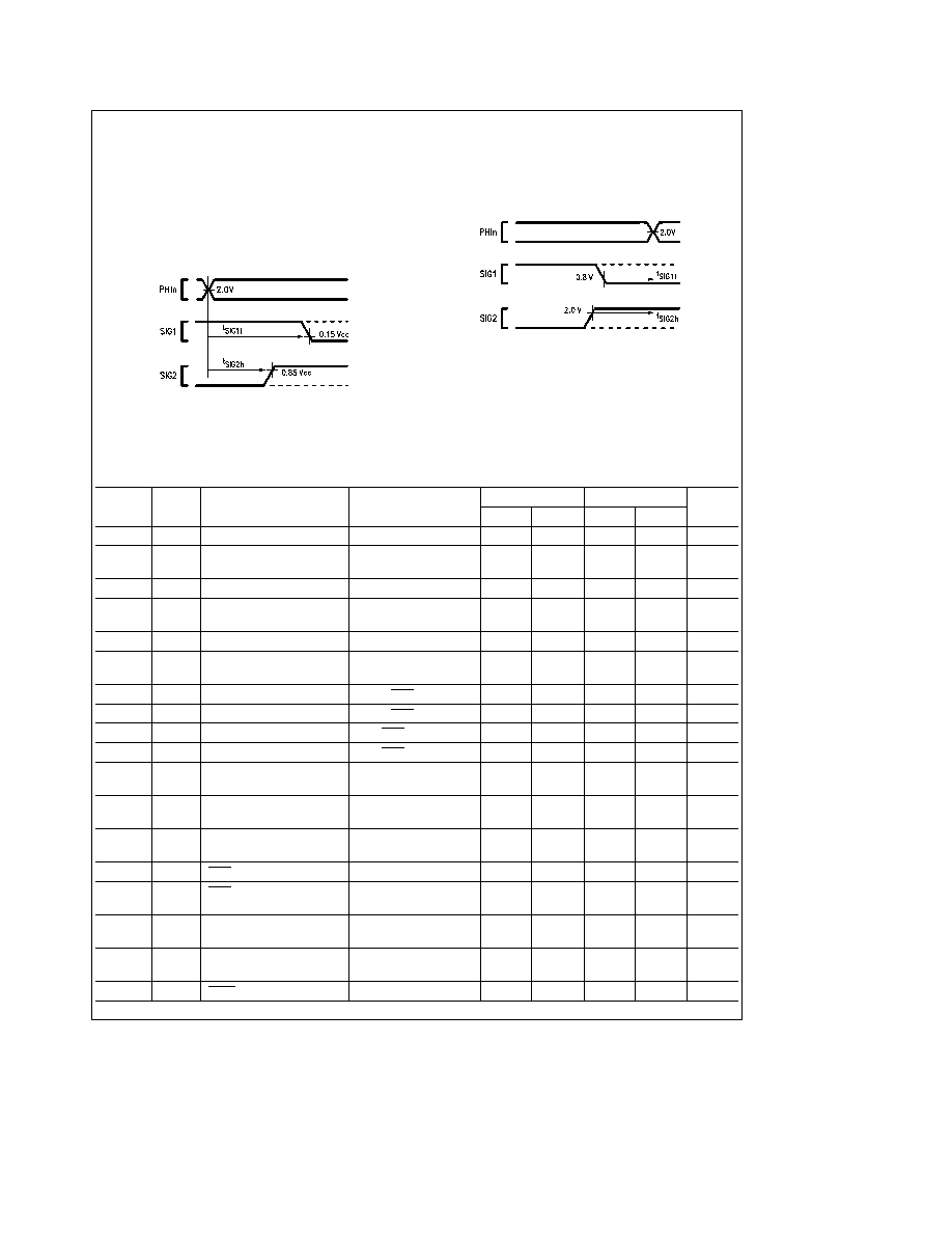
4 0 Device Specifications
(Continued)
4 4 SWITCHING CHARACTERISTICS
4 4 1 Definitions
All the timing specifications given in this section refer to
2 0V on the rising or falling edges of the clock phases PHI1
and PHI2 to 15% or 85% of V
CC
on all the CMOS output
signals and to 0 8V or 2 0V on all the TTL input signals as
illustrated in
Figures 4-2 and 4-3 unless specifically stated
otherwise
TL EE 8525 � 39
FIGURE 4-2 Timing Specification Standard
(CMOS Output Signals)
ABBREVIATIONS
L E
leading edge
R E
rising edge
T E
trailing edge
F E
falling edge
TL EE 8525 � 40
FIGURE 4-3 Timing Specification Standard
(TTL Input Signals)
4 4 2 Timing Tables
4 4 2 1 Output Signals Internal Propagation Delays NS32C016-10 and NS32C016-15
Maximum times assume capacitive loading of 75 pF on the address data bus signals and 50 pF on all other signals
Name
Figure
Description
Reference Conditions
NS32C016-10
NS32C016-15
Units
Min
Max
Min
Max
t
ALv
4-4
Address bits 0 � 15 valid
after R E PHI1 T1
40
35
ns
t
ALh
4-4
Address bits 0 � 15 hold
after R E PHI1
5
5
ns
Tmmu or T2
t
Dv
4-4
Data valid (write cycle)
after R E PHI1 T2
50
35
ns
t
Dh
4-4
Data hold (write cycle)
after R E PHI1
0
0
ns
next T1 or Ti
t
AHv
4-4
Address bits 16 � 23 valid
after R E PHI1 T1
40
35
ns
t
AHh
4-4
Address bits 16 � 23 hold
after R E PHI1
0
0
ns
next T1 or Ti
t
ALADSs
4-5
Address bits 0 � 15 set up
before ADS T E
25
20
ns
t
AHADSs
4-5
Address bits 16 � 23 set up
before ADS T E
25
20
ns
t
ALADSh
4-9
Address bits 0 � 15 hold
after ADS T E
15
10
ns
t
AHADSh
4-9
Address bits 16 � 23 hold
after ADS T E
15
10
ns
t
ALf
4-5
Address bits 0 � 15 floating
after R E PHI1 T2
25
20
ns
(no MMU)
t
ALMf
4-9
Address bits 0 � 15 floating
after R E PHI1 TMMU
25
20
ns
(with MMU)
t
AHMf
4-9
Address bits 16 � 23 floating
after R E PHI1 TMMU
25
20
ns
(with MMU)
t
HBEv
4-4
HBE signal valid
after R E PHI1 T1
45
35
ns
t
HBEh
4-4
HBE signal hold
after R E PHI1
0
0
ns
next T1 or Ti
t
STv
4-4
Status (ST0 � ST3) valid
after R E PHI1 T4
45
35
ns
(before T1 see note)
t
STh
4-4
Status (ST0 � ST3) hold
after R E PHI1 T4
0
0
ns
(after T1)
t
DDINv
4-5
DDIN signal valid
after R E PHI1 T1
50
35
ns
48
4 0 Device Specifications
(Continued)
4 4 2 1 Output Signals Internal Propagation Delays NS32C016-10 and NS32C016-15
(Continued)
Name
Figure
Description
Reference Conditions
NS32C016-10
NS32C016-15
Units
Min
Max
Min
Max
t
DDINh
4-5
DDIN signal hold
after R E PHI1
0
0
ns
next T1 or Ti
t
ADSa
4-4
ADS signal active (low)
after R E PHI1 T1
35
26
ns
t
ADSia
4-4
ADS signal inactive
after R E PHI2 T1
40
30
ns
t
ADSw
4-4
ADS pulse width
at 15% V
CC
(both edges)
30
25
ns
t
DSa
4-4
DS signal active (low)
after R E PHI1 T2
40
30
ns
t
DSia
4-4
DS signal inactive
after R E PHI1 T4
40
30
ns
t
ALf
4-6
AD0 � AD15 floating
after R E PHI1 T1
25
20
ns
(caused by HOLD)
t
AHf
4-6
A16 � A23 floating
after R E PHI1 T1
25
20
ns
(caused by HOLD)
t
DSf
4-6
DS floating (caused by HOLD)
after R E PHI1 Ti
50
40
ns
t
ADSf
4-6
ADS floating (caused by HOLD)
after R E PHI1 Ti
50
40
ns
t
HBEf
4-6
HBE floating (caused by HOLD)
after R E PHI1 Ti
50
40
ns
t
DDINf
4-6
DDIN floating (caused by HOLD)
after R E PHI1 Ti
50
40
ns
t
HLDAa
4-6
HLDA signal active (low)
after R E PHI1 Ti
30
25
ns
t
HLDAia
4-8
HLDA signal inactive
after R E PHI1 Ti
40
30
ns
t
DSr
4-8
DS signal returns from floating
after R E PHI1 Ti
55
40
ns
(caused by HOLD)
t
ADSr
4-8
ADS signal returns from floating
after R E PHI1 Ti
55
40
ns
(caused by HOLD)
t
HBEr
4-8
HBE signal returns from floating
after R E PHI1 Ti
55
40
ns
(caused by HOLD)
t
DDINr
4-8
DDIN signal returns from floating
after R E PHI1 Ti
55
40
ns
(caused by HOLD)
t
DDINf
4-9
DDIN signal floating (caused by FLT) after FLT F E
55
50
ns
t
HBEI
4-9
HBE signal low (caused by FLT)
after FLT F E
40
30
ns
t
DDINr
4-10
DDIN signal returns from floating
after FLT R E
40
30
ns
(caused by FLT)
t
HBEr
4-10
HBE signal returns from low
after FLT R E
35
25
ns
(caused by FLT)
t
SPCa
4-13
SPC output active (low)
after R E PHI1 T1
35
26
ns
t
SPCia
4-13
SPC output inactive
after R E PHI1 T4
35
26
ns
t
SPCnf
4-15
SPC output nonforcing
after R E PHI2 T4
30
25
ns
t
Dv
4-13
Data valid (slave processor write)
after R E PHI1 T1
50
35
ns
t
Dh
4-13
Data hold (slave processor write)
after R E PHI1 next T1 or Ti
0
0
ns
t
PFSw
4-18
PFS pulse width
at 15% V
CC
(both edges)
50
40
ns
t
PFSa
4-18
PFS pulse active (low)
after R E PHI2
40
35
ns
t
PFSia
4-18
PFS pulse inactive
after R E PHI2
40
35
ns
t
ILOs
4-20a
ILO signal setup
before R E PHI1 T1 of first
50
35
ns
interlocked write cycle
t
ILOh
4-20b
ILO signal hold
after R E PHI1 T3 of last
10
7
ns
interlocked read cycle
t
ILOa
4-21
ILO signal active (low)
after R E PHI1
35
30
ns
49
4 0 Device Specifications
(Continued)
4 4 2 1 Output Signals Internal Propagation Delays NS32C016-10 and NS32C016-15
(Continued)
Name
Figure
Description
Reference Conditions
NS32C016-10
NS32C016-15
Units
Min
Max
Min
Max
t
ILOia
4-21
ILO signal inactive
after R E PHI1
35
30
ns
t
USV
4-22
U S signal valid
after R E PHI1 T4
35
30
ns
t
USh
4-22
U S signal hold
after R E PHI1 T4
8
6
ns
t
NSPF
4-19b
Nonsequential fetch to
after R E PHI1 T1
4
4
t
Cp
next PFS clock cycle
t
PFNS
4-19a
PFS clock cycle to next
before R E PHI1 T1
4
4
t
Cp
nonsequential fetch
t
LXPF
4-29
Last operand transfer of
before R E PHI1 T1 of first
an instruction to next
bus cycle of transfer
0
0
t
Cp
PFS clock cycle
Note
Every memory cycle starts with T4 during which Cycle Status is applied If the CPU was idling the sequence will be ``
Ti T4 T1
'' If the CPU was
not idling the sequence will be ``
T4 T1
''
4 4 2 2 Input Signal Requirements NS32C016-10 and NS32C016-15
Name
Figure
Description
Reference Conditions
NS32C016-10
NS32C016-15
Units
Min
Max
Min
Max
t
PWR
4-25
Power stable to RST R E
after V
CC
reaches 4 5V
50
33
m
s
t
DIs
4-5
Data in setup (read cycle)
before F E PHI2 T3
15
10
ns
t
DIh
4-5
Data in hold (read cycle)
after F E PHI1 T4
3
3
ns
t
HLDa
4-6
HOLD active (low) setup
before F E PHI2 TX1
25
17
ns
time (see note)
t
HLDia
4-8
HOLD inactive setup time
before F E PHI2 Ti
25
17
ns
t
HLDh
4-6
HOLD hold time
after R E PHI1 TX2
0
0
ns
t
FLTa
4-9
FLT active (low) setup time
before F E PHI2 Tmmu
25
17
ns
t
FLTia
4-10
FLT inactive setup time
before F E PHI2 T2
25
17
ns
t
RDYs
4-11 4-12
RDY setup time
before F E PHI2 T2 or T3
15
10
ns
t
RDYh
4-11 4-12
RDY hold time
after F E PHI1 T3
5
5
ns
t
ABTs
4-23
ABT setup time
before F E PHI2 Tmmu
20
13
ns
(FLT inactive)
t
ABTs
4-24
ABT setup time
before F E PHI2 Tf
20
13
ns
(FLT active)
t
ABTh
4-23
ABT hold time
after R E PHI1
0
0
ns
t
RSTs
4-25 4-26
RST setup time
before F E PHI1
10
8
ns
t
RSTw
4-26
RST pulse width
at 0 8V (both edges)
64
64
t
Cp
t
INTs
4-27
INT setup time
before R E PHI1
20
15
ns
t
NMIw
4-28
NMI pulse width
at 0 8V (both edges)
70
70
ns
t
DIs
4-14
Data setup
before F E PHI2 T1
15
10
ns
(slave read cycle)
t
DIh
4-14
Data hold
after R E PHI1 T4
3
3
ns
(slave read cycle)
50
4 0 Device Specifications
(Continued)
4 4 2 2 Input Signal Requirements NS32C016-10 and NS32C016-15
(Continued)
Name
Figure
Description
Reference Conditions
NS32C016-10
NS32C016-15
Units
Min
Max
Min
Max
t
SPCd
4-15
SPC pulse delay
after R E PHI2 T4
30
25
ns
from slave
t
SPCs
4-15
SPC setup time
before F E PHI1
30
25
ns
t
SPCw
4-15
SPC pulse width from
at 0 8V (both edges)
slave processor
20
20
ns
(async input)
t
ATs
4-16
AT SPC setup for
before R E PHI1 of cycle
address translation
during which RST pulse
1
1
t
Cp
strap
is removed
t
ATh
4-16
AT SPC hold for
after F E PHI1 of cycle
address translation
during which RST pulse
2
2
t
Cp
strap
is removed
Note
This setup time is necessary to ensure prompt acknowledgement via HLDA and the ensuing floating of CPU off the buses Note that the time from the receipt
of the HOLD signal until the CPU floats is a function of the time HOLD signal goes low the state of the RDY input (in MMU systems) and the length of the current
MMU cycle
4 4 2 3 Clocking Requirements NS32C016-10 and NS32C016-15
Name
Figure
Description
Reference Conditions
NS32C016-10
NS32C016-15
Units
Min
Max
Min
Max
t
Cp
4-17
Clock period
R E PHI1 PHI2 to
100
250
66
250
ns
next R E PHI1 PHI2
t
CLw
4-17
PHI1 PHI2
At 2 0V
0 5t
Cp
0 5t
Cp
pulse width
on PHI1 PHI2
b
10 ns
b
6 ns
(both edges)
t
CLh
4-17
PHI1 PHI2
At 90% V
CC
0 5t
Cp
0 5t
Cp
High Time
on PHI1 PHI2
b
15 ns
b
10 ns
t
CLl
4-17
PHI1 PHI2
At 15% V
CC
0 5t
Cp
0 5t
Cp
Low Time
on PHI1 PHI2
b
5 ns
b
5 ns
t
nOVL(1 2)
4-17
Non-overlap time
At 15% V
CC
b
2
2
b
2
2
ns
on PHI1 PHI2
t
nOVLas
Non-overlap asymmetry
At 15% V
CC
b
3
3
b
3
3
ns
(t
nOVL(1)
b
t
nOVL(2)
)
on PHI1 PHI2
t
CLwas
PHI1 PHI2 asymmetry
At 2 0V
b
5
5
b
3
3
ns
(t
CLw(1)
b
t
CLw(2)
)
on PHI1 PHI2
51

4 0 Device Specifications
(Continued)
4 4 3 Timing Diagrams
TL EE 8525 � 41
FIGURE 4-4 Write Cycle
TL EE 8525 � 42
FIGURE 4-5 Read Cycle
52

4 0 Device Specifications
(Continued)
TL EE 8525 � 43
FIGURE 4-6 Floating by HOLD Timing (CPU Not Idle Initially)
Note that whenever the CPU is not idling (not in Ti) the HOLD request (HOLD low) must be active t
HLDa
before the falling edge of PHI2 of the clock cycle that
appears two clock cycles before T4 (TX1) and stay low until t
HLDh
after the rising edge of PHI1 of the clock cycle that precedes T4 (TX2) for the request to be
acknowledged
TL EE 8525 � 44
FIGURE 4-7 Floating by HOLD Timing (CPU Initially Idle)
Note that during Ti1 the CPU is already idling
TL EE 8525 � 80
FIGURE 4-8 Release from HOLD
53
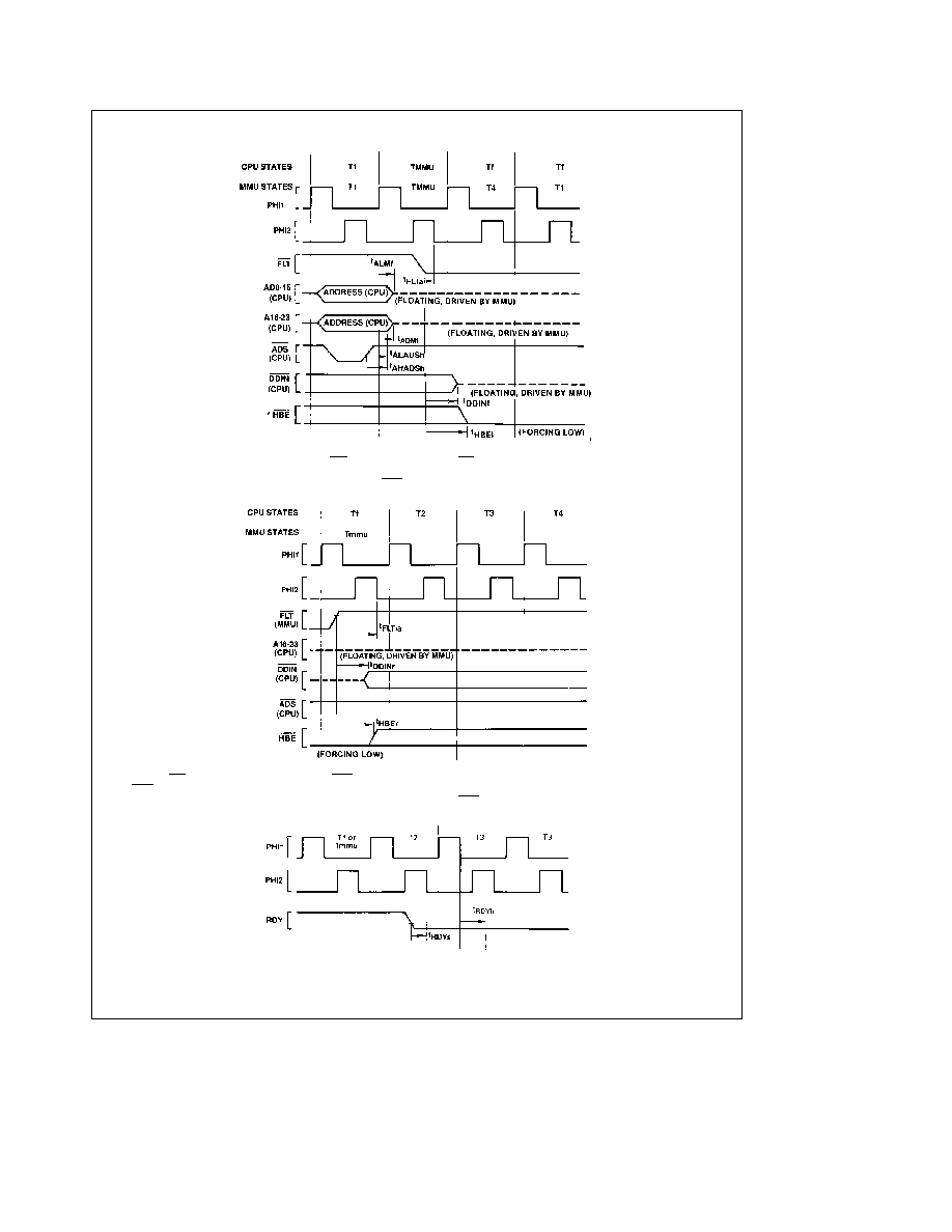
4 0 Device Specifications
(Continued)
TL EE 8525 � 46
Note In future higher speed versions of the NS32C016 HBE will no longer be affected by FLT See
Figure B-1 in Appendix B for the required modification to the
interface logic
FIGURE 4-9 FLT Initiated Cycle Timing
TL EE 8525 � 47
Note that when FLT is deasserted the CPU restarts driving DDIN before the MMU releases it This however does not cause any conflict since both CPU and MMU
force DDIN to the same logic level
FIGURE 4-10 Release from FLT Timing
TL EE 8525 � 48
FIGURE 4-11 Ready Sampling (CPU Initially READY)
54
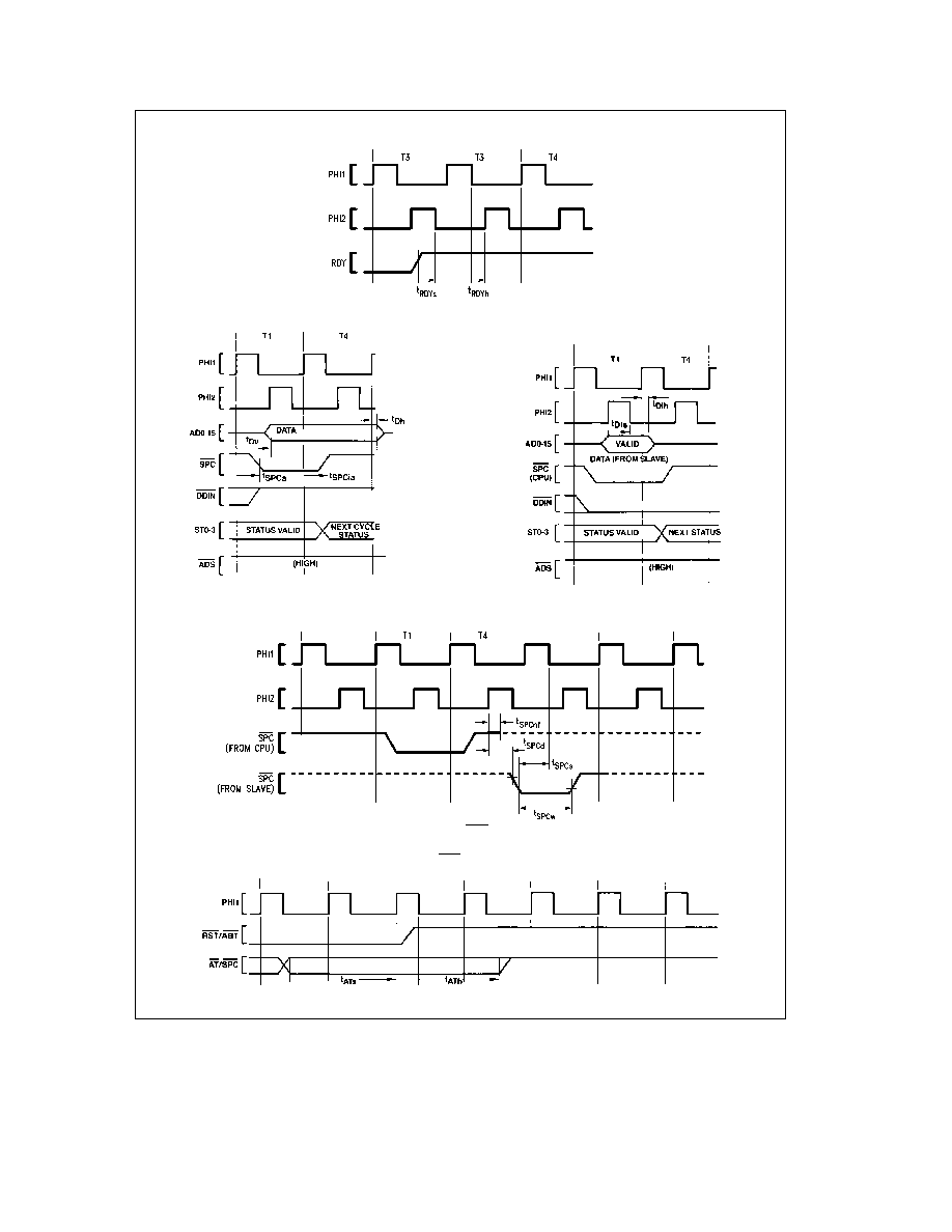
4 0 Device Specifications
(Continued)
TL EE 8525 � 49
FIGURE 4-12 Ready Sampling (CPU Initially NOT READY)
TL EE 8525 � 50
TL EE 8525 � 51
FIGURE 4-13 Slave Processor Write Timing
FIGURE 4-14 Slave Processor Read Timing
TL EE 8525 � 81
FIGURE 4-15 SPC Timing
After transferring last operand to a Slave Processor CPU turns
OFF driver and holds SPC high with internal 5 kX pullup
TL EE 8525 � 53
FIGURE 4-16 Reset Configuration Timing
55
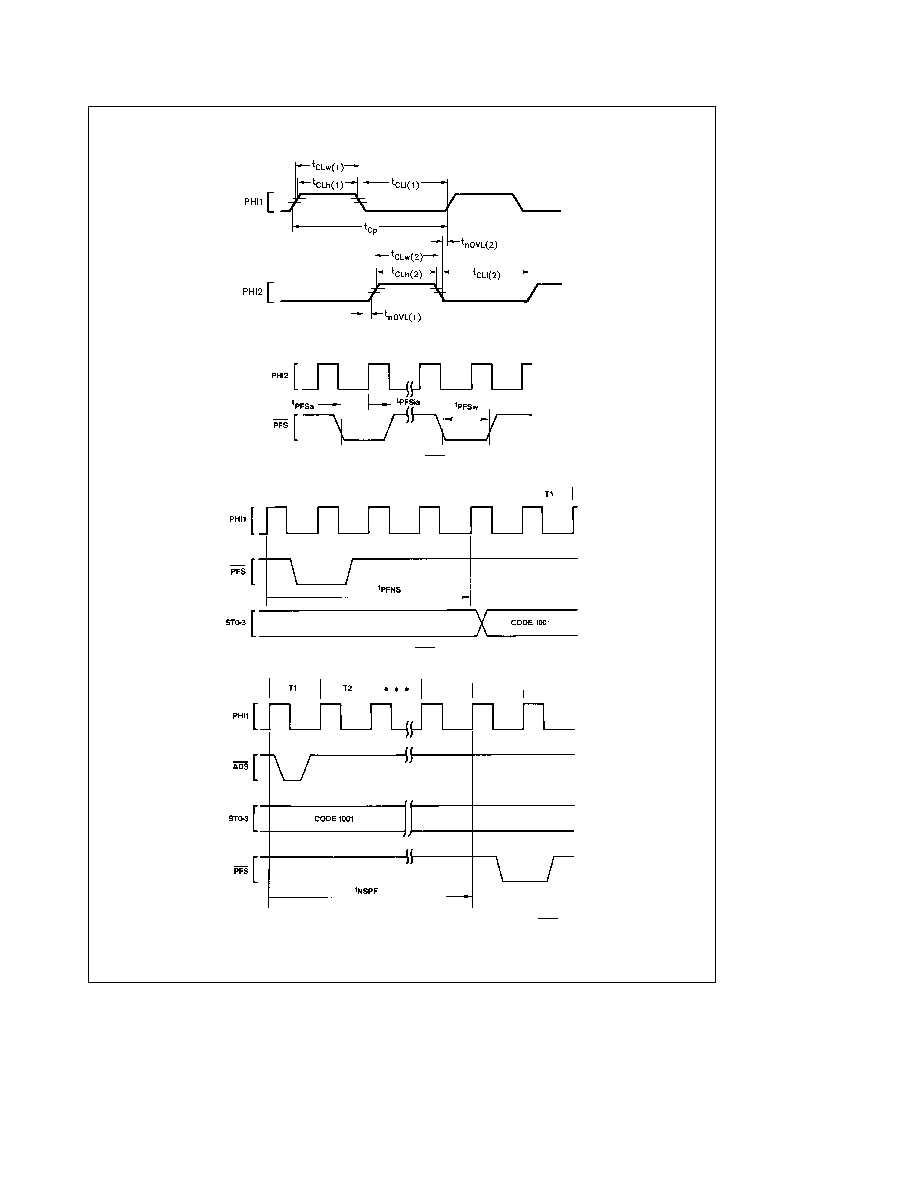
4 0 Device Specifications
(Continued)
TL EE 8525 � 54
FIGURE 4-17 Clock Waveforms
TL EE 8525 � 55
FIGURE 4-18 Relationship of PFS to Clock Cycles
TL EE 8525 � 56
FIGURE 4-19a Guaranteed Delay PFS to Non-Sequential Fetch
TL EE 8525 � 57
FIGURE 4-19b Guaranteed Delay Non-Sequential Fetch to PFS
56
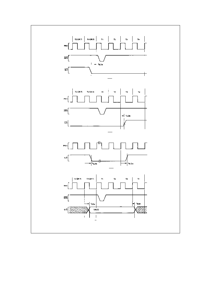
4 0 Device Specifications
(Continued)
TL EE 8525 � 58
FIGURE 4-20a Relationship of ILO to First Operand Cycle
of an Interlocked Instruction
TL EE 8525 � 59
FIGURE 4-20b Relationship of ILO to Last Operand Cycle
of an Interlocked Instruction
TL EE 8525 � 60
FIGURE 4-21 Relationship of ILO to Any Clock Cycle
TL EE 8525 � 61
FIGURE 4-22 U S Relationship to Any Bus Cycle
Guaranteed Valid Interval
57
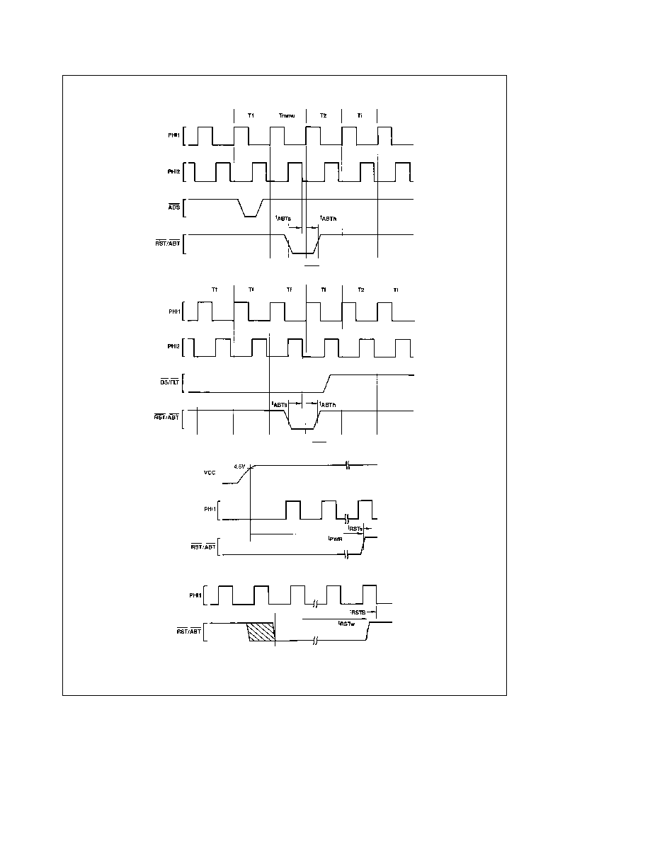
4 0 Device Specifications
(Continued)
TL EE 8525 � 62
FIGURE 4-23 Abort Timing FLT Not Applied
TL EE 8525 � 63
FIGURE 4-24 Abort Timing FLT Applied
TL EE 8525 � 64
FIGURE 4-25 Power-On Reset
TL EE 8525 � 65
FIGURE 4-26 Non-Power-On Reset
58
4 0 Device Specifications
(Continued)
TL EE 8525 � 66
FIGURE 4-27 INT Interrupt Signal Detection
TL EE 8525 � 67
FIGURE 4-28 NMI Interrupt Signal Timing
TL EE 8525 � 68
FIGURE 4-29 Relationship Between Last Data Transfer of
an Instruction and PFS Pulse of Next Instruction
NOTE
In a transfer of a Read-Modify-Write type operand this is the Read transfer
displaying RMW Status (Code 1011)
59
Appendix A Instruction Formats
NOTATIONS
i
e
Integer Type Field
B
e
00 (Byte)
W
e
01 (Word)
D
e
11 (Double Word)
f
e
Floating Point Type Field
F
e
1 (Std Floating 32 bits)
L
e
0 (Long Floating 64 bits)
c
e
Custom Type Field
D
e
1 (Double Word)
Q
e
0 (Quad Word)
op
e
Operation Code
Valid encodings shown with each format
gen gen 1 gen 2
e
General Addressing Mode Field
See Sec 2 2 for encodings
reg
e
General Purpose Register Number
cond
e
Condition Code Field
0000
e
EQual Z
e
1
0001
e
Not Equal Z
e
0
0010
e
Carry Set C
e
1
0011
e
Carry Clear C
e
0
0100
e
Higher L
e
1
0101
e
Lower or Same L
e
0
0110
e
Greater Than N
e
1
0111
e
Less or Equal N
e
0
1000
e
Flag Set F
e
1
1001
e
Flag Clear F
e
0
1010
e
LOwer L
e
0 and Z
e
0
1011
e
Higher or Same L
e
1 or Z
e
1
1100
e
Less Than N
e
0 and Z
e
0
1101
e
Greater or Equal N
e
1 or Z
e
1
1110
e
(Unconditionally True)
1111
e
(Unconditionally False)
short
e
Short Immediate Value May contain
quick Signed 4-bit value in MOVQ ADDQ
CMPQ ACB
cond Condition Code (above) in Scond
areg
CPU Dedicated Register in LPR SPR
0000
e
US
0001
b
0111
e
(Reserved)
1000
e
FP
1001
e
SP
1010
e
SB
1011
e
(Reserved)
1100
e
(Reserved)
1101
e
PSR
1110
e
INTBASE
1111
e
MOD
Options in String Instructions
U W
B
T
T
e
Translated
B
e
Backward
U W
e
00 None
01 While Match
11 Until Match
Configuration bits in SETCFG
C
M
F
I
mreg
NS32082 Register number in LMR SMR
0000
e
BPR0
0001
e
BPR1
0010
e
(Reserved)
0011
e
(Reserved)
0100
e
(Reserved)
0101
e
(Reserved)
0110
e
(Reserved)
0111
e
(Reserved)
1000
e
(Reserved)
1001
e
(Reserved)
1010
e
MSR
1011
e
BCNT
1100
e
PTB0
1101
e
PTB1
1110
e
(Reserved)
1111
e
EIA
7
0
cond
1 0 1 0
Format 0
Bcond
(BR)
7
0
op
0 0 1 0
Format 1
BSR
b
0000
ENTER
b
1000
RET
b
0001
EXIT
b
1001
CXP
b
0010
NOP
b
1010
RXP
b
0011
WAIT
b
1011
RETT
b
0100
DIA
b
1100
RETI
b
0101
FLAG
b
1101
SAVE
b
0110
SVC
b
1110
RESTORE
b
0111
BPT
b
1111
15
8
7
0
gen
short
op
1
1
i
Format 2
ADDQ
b
000
ACB
b
100
CMPQ
b
001
MOVQ
b
101
SPR
b
010
LPR
b
110
Scond
b
011
60
Appendix A Instruction Formats
(Continued)
15
8 7
0
gen
op
1 1 1 1 1
i
Format 3
CXPD
b
0000
ADJSP
b
1010
BICPSR
b
0010
JSR
b
1100
JUMP
b
0100
CASE
b
1110
BISPSR
b
0110
Trap (UND) on XXX1 1000
15
8 7
0
gen 1
gen 2
op
i
Format 4
ADD
b
0000
SUB
b
1000
CMP
b
0001
ADDR
b
1001
BIC
b
0010
AND
b
1010
ADDC
b
0100
SUBC
b
1100
MOV
b
0101
TBIT
b
1101
OR
b
0110
XOR
b
1110
23
16 15
8 7
0
0 0 0 0 0
short
0
op
i
0 0 0 0 1 1 1 0
Format 5
MOVS
b
0000
SETCFG
b
0010
CMPS
b
0001
SKPS
b
0011
Trap (UND) on 1XXX 01XX
23
16 15
8 7
0
gen 1
gen 2
op
i
0 1 0 0 1 1 1 0
Format 6
ROT
b
0000
NEG
b
1000
ASH
b
0001
NOT
b
1001
CBIT
b
0010
Trap (UND)
b
1010
CBITI
b
0011
SUBP
b
1011
Trap (UND)
b
0100
ABS
b
1100
LSH
b
0101
COM
b
1101
SBIT
b
0110
IBIT
b
1110
SBITI
b
0111
ADDP
b
1111
23
16 15
8 7
0
gen 1
gen 2
op
i
1 1 0 0 1 1 1 0
Format 7
MOVM
b
0000
MUL
b
1000
CMPM
b
0001
MEI
b
1001
INSS
b
0010
Trap (UND)
b
1010
EXTS
b
0011
DEI
b
1011
MOVXBW
b
0100
QUO
b
1100
MOVZBW
b
0101
REM
b
1101
MOVZiD
b
0110
MOD
b
1110
MOVXiD
b
0111
DIV
b
1111
TL EE 8525 � 69
Format 8
EXT
b
000
INDEX
b
100
CVTP
b
001
FFS
b
101
INS
b
010
CHECK
b
011
MOVSU
b
110 reg
e
001
MOVUS
b
110 reg
e
011
23
16 15
8 7
0
gen 1
gen 2
op
f
i
0 0 1 1 1 1 1 0
Format 9
MOVif
b
000
ROUND
b
100
LFSR
b
001
TRUNC
b
101
MOVLF
b
010
SFSR
b
110
MOVFL
b
011
FLOOR
b
111
TL EE 8525 � 70
Format 10
Trap (UND) Always
61

Appendix A Instruction Formats
(Continued)
23
16 15
8 7
0
gen 1
gen 2
op
0 f 1 0 1 1 1 1 1 0
Format 11
ADDf
b
0000
DIVf
b
1000
MOVf
b
0001
Trap (SLAVE)
b
1001
CMPf
b
0010
Trap (UND)
b
1010
Trap (SLAVE)
b
0011
Trap (UND)
b
1011
SUBf
b
0100
MULf
b
1100
NEGf
b
0101
ABSf
b
1101
Trap (UND)
b
0110
Trap (UND)
b
1110
Trap (UND)
b
0111
Trap (UND)
b
1111
TL EE 8525 � 71
Format 12
Trap (UND) Always
TL EE 8525 � 72
Format 13
Trap (UND) Always
23
16 15
8 7
0
gen 1
short
0
op
i
0 0 0 1 1 1 1 0
Format 14
RDVAL
b
0000
LMR
b
0010
WRVAL
b
0001
SMR
b
0011
Trap (UND) on 01XX 1XXX
23
16 15
8 7
0
n n n 1 0 1 1 0
Operation Word
ID Byte
Format 15
(Custom Slave)
nnn
Operation Word Format
23
16 15
8
000
gen 1
short
x
op
i
Format 15 0
CATST0
b
0000
LCR
b
0010
CATST1
b
0001
SCR
b
0011
Trap (UND) on all others
23
16 15
8
001
gen 1
gen 2
op c
i
Format 15 1
CCV3
b
000
CCV2
b
100
LCSR
b
001
CCV1
b
101
CCV5
b
010
SCSR
b
110
CCV4
b
011
CCV0
b
111
23
16 15
8
101
gen 1
gen 2
op
x c
Format 15 5
CCAL0
b
0000
CCAL3
b
1000
CMOV0
b
0001
CMOV3
b
1001
CCMP0
b
0010
Trap (UND)
b
1010
CCMP1
b
0011
Trap (UND)
b
1011
CCAL1
b
0100
CCAL2
b
1100
CMOV2
b
0101
CMOV1
b
1101
Trap (UND)
b
0110
Trap (UND)
b
1110
Trap (UND)
b
0111
Trap (UND)
b
1111
If nnn
e
010 011 100 110 111
then Trap (UND) Always
62
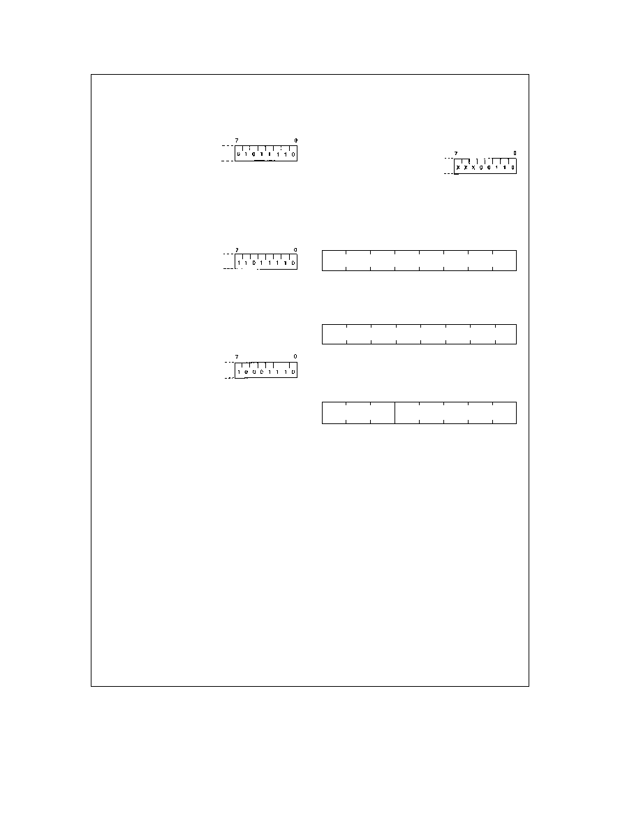
Appendix A Instruction Formats
(Continued)
TL EE 8525 � 73
Format 16
Trap (UND) Always
TL EE 8525 � 75
Format 17
Trap (UND) Always
TL EE 8525 � 76
Format 18
Trap (UND) Always
TL EE 8525 � 74
Format 19
Trap (UND) Always
Implied Immediate Encodings
7
0
r7
r6
r5
r4
r3
r2
r1
r0
Register Mask appended to SAVE ENTER
7
0
ro
r1
r2
r3
r4
r5
r6
r7
Register Mask appended to RESTORE EXIT
7
0
offset
length
b
1
Offset Length Modifier appended to INSS EXTS
63
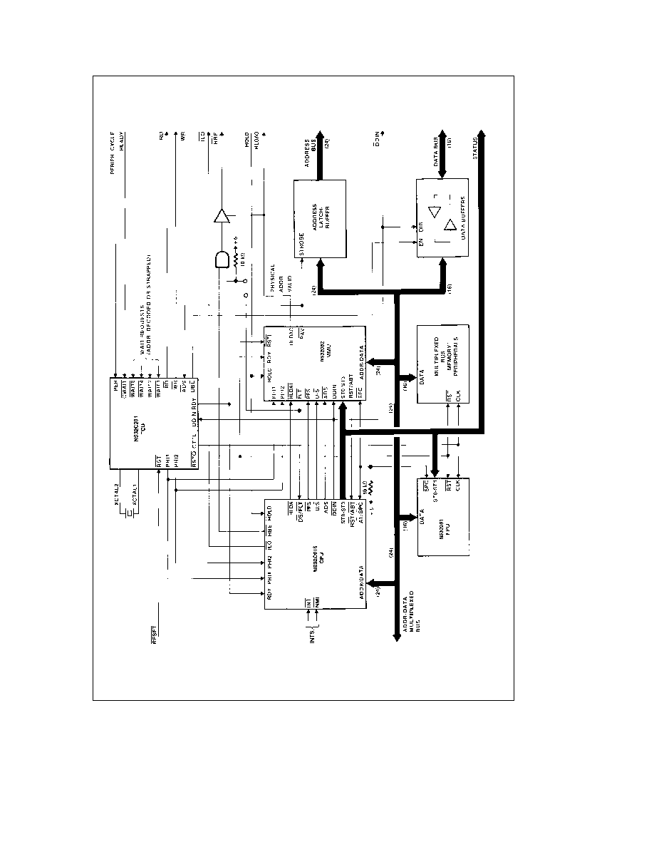
Appendix B Interfacing Suggestions
TLEE8525
�
7
7
FIGURE
B-1
System
Connection
Diagram
64

65
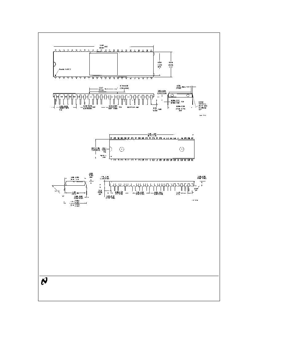
NS32C016-10NS32C016-15
High-Performance
Microprocessors
Physical Dimensions
inches (millimeters)
Lit
114273
Ceramic Dual-In-Line Package (D)
Order Number NS32C016D-10 or NS32C016D-15
NS Package Number D48A
Molded Dual-In-Line Package (N)
Order Number NS32C016N-10 or NS32C016N-15
NS Package Number N48A
LIFE SUPPORT POLICY
NATIONAL'S PRODUCTS ARE NOT AUTHORIZED FOR USE AS CRITICAL COMPONENTS IN LIFE SUPPORT
DEVICES OR SYSTEMS WITHOUT THE EXPRESS WRITTEN APPROVAL OF THE PRESIDENT OF NATIONAL
SEMICONDUCTOR CORPORATION As used herein
1 Life support devices or systems are devices or
2 A critical component is any component of a life
systems which (a) are intended for surgical implant
support device or system whose failure to perform can
into the body or (b) support or sustain life and whose
be reasonably expected to cause the failure of the life
failure to perform when properly used in accordance
support device or system or to affect its safety or
with instructions for use provided in the labeling can
effectiveness
be reasonably expected to result in a significant injury
to the user
National Semiconductor
National Semiconductor
National Semiconductor
National Semiconductor
Corporation
Europe
Hong Kong Ltd
Japan Ltd
1111 West Bardin Road
Fax (a49) 0-180-530 85 86
13th Floor Straight Block
Tel 81-043-299-2309
Arlington TX 76017
Email cnjwge tevm2 nsc com
Ocean Centre 5 Canton Rd
Fax 81-043-299-2408
Tel 1(800) 272-9959
Deutsch Tel (a49) 0-180-530 85 85
Tsimshatsui Kowloon
Fax 1(800) 737-7018
English
Tel (a49) 0-180-532 78 32
Hong Kong
Fran ais Tel (a49) 0-180-532 93 58
Tel (852) 2737-1600
Italiano
Tel (a49) 0-180-534 16 80
Fax (852) 2736-9960
National does not assume any responsibility for use of any circuitry described no circuit patent licenses are implied and National reserves the right at any time without notice to change said circuitry and specifications