TL EE11331
NS32FX100-15NS32FX100-20NS32FV100-20NS32FV100-25
NS32FX200-20NS32FX200-25
System
Controller
PRELIMINARY
July 1992
NS32FX100-15 NS32FX100-20 NS32FV100-20
NS32FV100-25 NS32FX200-20 NS32FX200-25
System Controller
General Description
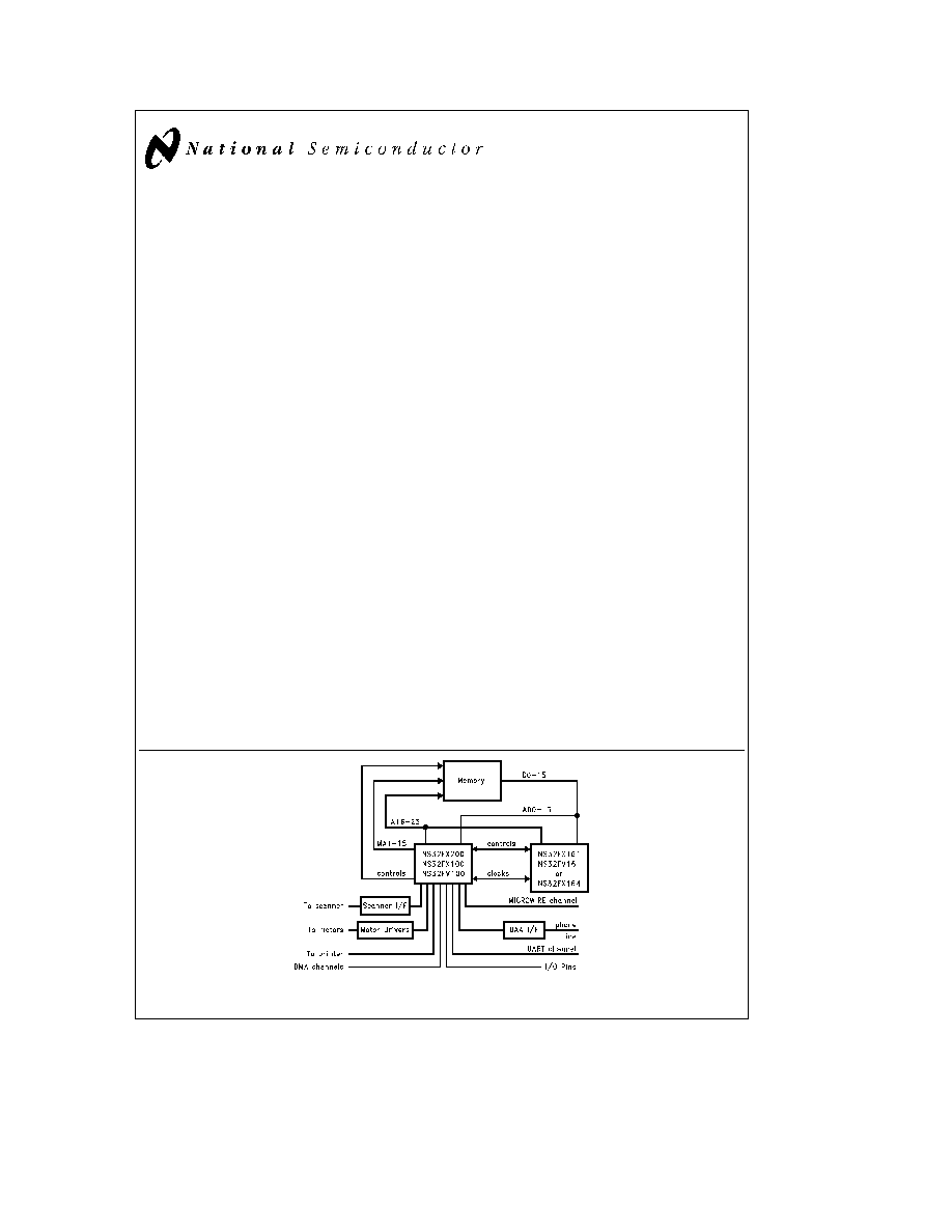
The NS32FX200 NS32FV100 and NS32FX100 are highly
integrated system chips designed for a FAX system based
on National Semiconductor's embedded processors
NS32FX161 NS32FV16 or NS32FX164 The NS32FX100 is
the common core for all three system chips
The
NS32FV100 and NS32FX200 offer additional functions
Throughout this document references to the NS32FX100
also apply to both the NS32FV100 and the NS32FX200
Specific NS32FV100 or NS32FX200 features are explicitly
indicated
The NS32FX200 NS32FV100 and NS32FX100 feature an
interface to devices like stepper motors printers and scan-
ners a Sigma-Delta CODEC an elapsed-time counter a
DMA controller an interrupt controller and a UART
The NS32FX200 is optimized for high-end FAX applications
such as plain-paper FAX and multifunctional peripherals
The NS32FX100 is optimized for low-cost FAX applica-
tions The NS32FV100 is optimized for thermal paper FAX
machines with Digital Answering Machine support
Features
Y
Direct interface to the NS32FX161
NS32FV16 and
NS32FX164 embedded processors
Y
Supports a variety of Contact Image Sensor (CIS) and
Charge Coupled Device (CCD) scanners
Y
Direct interface to a variety of Thermal Print Head
(TPH) printers Bitmap shifter and DMA channels facili-
tate the connection of other types of printers
Y
Supports two stepper motors
Y
Direct interface to ROM and SRAM The NS32FX200
and NS32FV100 in addition interface to DRAM
devices
Y
Programmable wait state generator
Y
Demultiplexed address and data buses
Y
Multiplexed
DRAM
address
bus
(NS32FX200
and
NS32FV100)
Y
Supports 3V freeze mode by maintaining only elapsed
time counter
Y
Control of power consumption by disabling inactive
modules and reducing the clock frequency
Y
Operating frequency
Normal mode 19 6608 MHz
24 576 MHz in steps
of 1 2288 MHz (NS32FX200)
Normal mode 19 6608 MHz
24 576 MHz in steps
of 1 2288 MHz (NS32FV100)
Normal mode 14 7456 MHz
19 6608 MHz in steps
of 1 2288 MHz (NS32FX100)
Power Save mode Normal mode frequency divided
by sixteen
Y
On-Chip full duplex Sigma-Delta CODEC with
Total harmonic distortion better than
b
70 dB
Programmable hybrid balance filter
Programmable reception and transmission filters
Programmable gain control
Y
On-Chip Interrupt Control Unit with
16 interrupt sources
Programmable triggering mode
Y
On-Chip counters WATCHDOG
TM
UART
MICROWIRE
TM
System Clock Generator and I O
ports
Y
On-Chip DMA controller (NS32FX200
four channels
NS32FX100 NS32FV100
three channels)
Y
Up to 37 on-chip general purpose I O pins expandable
externally
Y
Flexible allocation of I O and modules' pins
Y
132-pin JEDEC PQFP package
TL EE 11331 � 1
FIGURE 1-1 A FAX Controller Block Diagram
TRI-STATE
is a registered trademark of National Semiconductor Corporation
MICROWIRE
TM
and WATCHDOG
TM
are trademarks of National Semiconductor Corporation
C1995 National Semiconductor Corporation
RRD-B30M105 Printed in U S A

Table of Contents
1 0 FAX SYSTEM CONFIGURATION
6
1 1 Block Diagram Description
6
1 2 Module Diagram
7
1 2 1 Bus and Memory Controller (BMC)
8
1 2 2 Timing Control Unit (TCU)
8
1 2 3 Sigma-Delta CODEC (SDC)
8
1 2 4 Scanner Controller (SCANC)
8
1 2 5 Printer Controller (PRNTC)
8
1 2 6 DMA Controller (DMAC)
8
1 2 7 Universal Asynchronous Receiver-Transmitter
(UART)
8
1 2 8 MICROWIRE (MWIRE)
8
1 2 9 Interrupt Control Unit (ICU)
8
1 2 10 Ports
8
1 3 Operation Modes
8
1 3 1 Functionality
9
2 0 ARCHITECTURE
10
2 1 MCFG
Module Configuration Register
10
2 2 Timing Control Unit (TCU)
10
2 2 1 Features
10
2 2 2 Operation
10
2 2 2 1 External Clocks
11
2 2 2 2 Internal Clocks
11
2 2 3 Registers
12
2 2 3 1 Usage Recommendations
13
2 3 Sigma-Delta CODEC (SDC)
13
2 3 1 Features
13
2 3 2 Operation
13
2 3 2 1 Block Diagram
13
2 3 2 2 On-Chip Digital Blocks
15
2 3 3 Programmable Functions
15
2 3 3 1 Sigma-Delta ON OFF
15
2 3 4 Off-Chip Analog Circuits
15
2 3 4 1 Analog Transmitter
17
2 3 4 2 Analog Receiver
17
2 3 5 Registers
17
2 3 6 Usage Recommendations
18
2 4 Scanner Controller (SCANC)
18
2 4 1 Features
18
2 4 2 Operation
18
2 4 2 1 Scanner Signals Generator Block
19
2 4 2 2 Scanner Period Pulse (SPP)
Generation
20
2 4 2 3 Video Handling Block
21
2 4 2 4 Threshold DAC (Dithering and
Automatic Background Control)
22
2 4 2 5 Stepper Motor Control Block
23
2 0 ARCHITECTURE
(Continued)
2 4 3 Registers
23
2 4 4 Usage Recommendations
24
2 5 Printer Controller (PRNTC)
25
2 5 1 Features
25
2 5 2 Operation
25
2 5 2 1 Printer Bitmap Shifter Block
25
2 5 2 2 Thermal Print-Head Control Block
25
2 5 3 Registers
28
2 5 4 Usage Recommendations
28
2 6 Direct Memory Access Controller (DMAC)
29
2 6 1 Features
29
2 6 2 Description
29
2 6 2 1 A General DMA Channel
29
2 6 2 2 Transfer Types
29
2 6 2 3 Operation Modes
29
2 6 3 Detailed Operation Flow
29
2 6 4 NS32FX200 DMA Channels
30
2 6 5 Registers
30
2 6 6 Usage Recommendations
32
2 6 7 DMAC Bus Cycles
32
2 7 Universal Asynchronous Receiver-Transmitter
(UART)
36
2 7 1 Features
36
2 7 2 Operation
36
2 7 3 Registers
37
2 7 4 Usage Recommendations
38
2 8 MICROWIRE (MWIRE)
38
2 8 1 Features
38
2 8 2 Operation
38
2 8 3 Registers
38
2 8 4 Usage Recommendations
40
2 9 Interrupt Control Unit (ICU)
40
2 9 1 Features
40
2 9 2 Operation
40
2 9 3 Registers
41
2 9 4 Usage Recommendations
41
2 10 Ports Module
41
2 10 1 Features
41
2 10 2 Operation
41
2 10 2 1 General Purpose Input Output
Ports
41
2 10 2 2 External Output Port Extension 43
2 10 2 3 Stepper Motors Output Ports
43
2 10 3 Registers
43
2 10 4 Usage Recommendations
45
2

Table of Contents
(Continued)
2 0 ARCHITECTURE
(Continued)
2 11 Bus and Memory Controller (BMC)
45
2 11 1 Features
45
2 11 2 Operation
45
2 11 2 1 Zones 0 1 (ROM and SRAM)
Transactions
46
2 11 2 2 Zone 2 (Dynamic Memory)
Transactions (NS32FX200 and
NS32FV100 only)
46
2 11 2 3 Zone 3 (I O) Transactions
47
2 11 2 4 Operation in Freeze Mode
47
2 11 2 5 On-Chip Registers Access
47
2 11 3 Registers
47
2 11 4 Usage Recommendations
48
2 12 Register Summary
48
2 12 1 NS32FX100 Registers Access Method
48
2 12 2 NS32FX200 NS32FV100 and NS32FX100
Registers
48
3 0 SYSTEM INTERFACE
53
3 1 Power and Grounding
53
3 2 Clocks and Traps Connectivity
53
3 0 SYSTEM INTERFACE
(Continued)
3 3 Control of Power Consumption
53
3 4 Bus Cycles
54
4 0 DEVICE SPECIFICATIONS
62
4 1 NS32FX100 Pin Descriptions
62
4 1 1 Supplies
62
4 1 2 Input Signals
62
4 1 3 Output Signals
63
4 1 4 Input Output Signals
64
4 2 Output Signal Levels
64
4 2 1 Freeze Mode Output Signals
65
4 2 2 Reset Power Restore Output Signals
65
4 3 Absolute Maximum Ratings
67
4 4 Electrical Characteristics
67
4 5 Analog Electrical Characteristics
69
4 6 Switching Characteristics
70
4 6 1 Definitions
70
4 6 2 Timing Tables
71
4 6 2 1 Output Signals Internal Propagation
Delays
71
4 6 2 2 Input Signal Requirements
76
APPENDIX A CODEC TRANSMISSION
PERFORMANCE
92
3

List of Figures
FIGURE 1-1
A FAX Controller Block Diagram
1
FIGURE 1-2
NS32FX100 Module Diagram
7
FIGURE 1-3
NS32FV100 Module Diagram
7
FIGURE 1-4
NS32FX200 Module Diagram
7
FIGURE 1-5
System Chip States and Operation Modes
9
FIGURE 2-1
Clocks and Traps Connectivity
10
FIGURE 2-2
High Speed Oscillator Clocks
11
FIGURE 2-3
Low Speed Oscillator Clocks
11
FIGURE 2-4
Sigma-Delta Block Diagram
14
FIGURE 2-5
SDC Off-Chip Analog Circuit
16
FIGURE 2-6
Block Diagram of Scanner's Signals Generator Block
19
FIGURE 2-7
Scanner Pixel Control Signals
20
FIGURE 2-8
Scanner Period Control Signals
21
FIGURE 2-9
Block Diagram of Scanner's Video Handling Block
21
FIGURE 2-10
Dither Cyclic Buffer
22
FIGURE 2-11
Bitmap Shifter Signals
25
FIGURE 2-12
Four Strobes Mode (STBM
e
00)
26
FIGURE 2-13
Two Strobes Mode (STBM
e
01)
26
FIGURE 2-14
Temperature ADC
27
FIGURE 2-15
DMA Fly-By Read Transaction (DIR
e
0 FBY
e
0)
32
FIGURE 2-16
DMA Fly-By Write Transaction (DIR
e
1 FBY
e
0)
33
FIGURE 2-17
DMA Memory to I O Read Transaction (DIR
e
0 NFBY
e
1)
34
FIGURE 2-18
DMA I O to Memory Write Transaction (DIR
e
1 NFBY
e
1)
35
FIGURE 2-19
Two Adjacent Fly-By DMA Transactions
36
FIGURE 2-20
Character Format
37
FIGURE 2-21
MICROWIRE Transaction (CLKM
e
0)
39
FIGURE 2-22
MICROWIRE Transaction (CLKM
e
1)
39
FIGURE 2-23
Port A
42
FIGURE 2-24
Port B
42
FIGURE 2-25
Port C
42
FIGURE 2-26
External Output Port Extension
43
FIGURE 3-1
Power and Ground Connections
53
FIGURE 3-2
Oscillator Circuits
53
FIGURE 3-3
Zones 0 1 (ROM SRAM) Read Transaction Zero Wait State
54
FIGURE 3-4
Zones 0 1 (ROM SRAM) Read Transaction One Wait State
54
FIGURE 3-5
Zones 0 1 (ROM SRAM) Write Transaction Zero Wait State
55
FIGURE 3-6
Zones 0 1 (ROM SRAM) Write Transaction One Wait State
55
FIGURE 3-7
Zone 2 (DRAM) Refresh Transaction Zero Wait State
56
FIGURE 3-8
Zone 2 (DRAM) Refresh Transaction Three Wait States
56
FIGURE 3-9
Freeze Mode Refresh Transaction Waveform
56
FIGURE 3-10
Zone 2 (DRAM) Read Transaction Zero Wait State
57
FIGURE 3-11
Zones 0 1 Access Delayed by a Refresh Transaction (No Wait)
57
FIGURE 3-12
Zone 2 (DRAM) Read Transaction One Wait State
58
FIGURE 3-13
Zone 2 (DRAM) Write Transaction Zero Wait State
58
FIGURE 3-14
Zone 2 (DRAM) Write Transaction One Wait State
59
FIGURE 3-15
Zone 3 (I O) Read Transaction Two Wait States
59
FIGURE 3-16
Zone 3 (I O) Read Transaction Four Wait States
60
FIGURE 3-17
Zone 3 (I O) Write Transaction Four Wait States
60
FIGURE 3-18
Zone 3 (I O) Write Transaction Six Wait States
61
FIGURE 3-19
CPU DMA Arbitration
61
FIGURE 3-20
Spaced Memory Transaction Two Tidles after T4
61
4

List of Figures
(Continued)
FIGURE 4-1
Connection Diagram
Top View
66
FIGURE 4-2
Analog Circuitry Block Diagram
69
FIGURE 4-3
TTL
Output Signals Specification Standard
70
FIGURE 4-4
TTL
Input Signals Specification Standard
70
FIGURE 4-5
CMOS
Output Signals Specification Standard
70
FIGURE 4-6
CMOS
Input Signals Specification Standard
70
FIGURE 4-7
Input Hysteresis
70
FIGURE 4-8
Clock Waveforms
79
FIGURE 4-9
DRAM Read Bus Cycle
79
FIGURE 4-10
DRAM Write Bus Cycle
80
FIGURE 4-11
ROM SRAM Read Bus Cycle
81
FIGURE 4-12
ROM SRAM Write Bus Cycle (One Wait State)
82
FIGURE 4-13
I O Read Bus Cycle
83
FIGURE 4-14
I O Write Bus Cycle
83
FIGURE 4-15
DRAM Refresh Bus Cycles
84
FIGURE 4-16
DMA Read Transaction (DIR
e
0)
85
FIGURE 4-17
DMA Write Transaction (DIR
e
1)
86
FIGURE 4-18
Interrupt Signals Timing
87
FIGURE 4-19
Sigma-Delta Signals Timing
87
FIGURE 4-20
SBYPS Input Signal Timing
87
FIGURE 4-21
Printer Signals Timing
88
FIGURE 4-22
Reset Signals Timing
88
FIGURE 4-23
Scanner Signals Timing
89
FIGURE 4-24
UART Signals Timing
90
FIGURE 4-25
MWIRE Signals Timing
90
FIGURE 4-26
Ports Signals Timing
91
FIGURE 4-27
Analog Signals Timing
91
List of Tables
TABLE 2-1
CTTL MCLON and MCLOFF Values
12
TABLE 2-2
Component Values
15
TABLE 2-3
Interrupt Sources and Priority Levels
40
TABLE 2-4
DRAM Address Multiplexing
46
TABLE 2-5
DRAM Address Sizes
46
TABLE 3-1
R C and L Values
53
TABLE 3-2
System Chip Operation Modes and Power Consumption
53
TABLE A-1
Transmitter Performance
92
TABLE A-2
Receiver Performance
93
5