TL EE11267
NS32FX161-15NS32FX161-20NS32FX164-20NS32FX164-25NS32FV16-20NS32FV16-25
Advanced
ImagingCommunication
Signal
Processors
February 1992
NS32FX161-15 NS32FX161-20 NS32FX164-20
NS32FX164-25 NS32FV16-20 NS32FV16-25
Advanced Imaging Communication Signal Processors
General Description
The NS32FX164 the NS32FV16 and the NS32FX161 are
high-performance 32-bit members of the Series 32000
EP
TM
family of National's Embedded System Processors
TM
specifically optimized for CCITT Group 2 and Group 3 Fac-
simile Applications Data Modems Voice Mail Systems La-
ser Printers or any combination of the above
Unless
specified
otherwise
any
reference
to
the
NS32FX164 in this document applies to the NS32FV16 and
the NS32FX161 as well
The NS32FX164 can perform all the computations and con-
trol functions required for a stand-alone Fax system a PC
add-in Fax Voice Data Modem card or a Laser Fax sys-
tem
It also meets the performance requirements to implement
14400 9600 and 7200 bps modems complying with CCITT
V 17 V 29 and V 27 standards The NS32FV16 supports
V 29 and V 27 standards as well as voice The NS32FX161
supports V 29 and V 27 standards
The NS32FX164 provides a 16 Mbyte Linear external ad-
dress space and a 16-bit external data bus
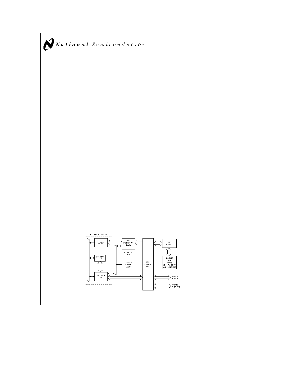
The CPU core which is the same as that of the NS32CG16
incorporates a 32-bit ALU and instruction pipeline and an
8-byte prefetch queue
Also integrated on-chip with the CPU are a DSP Module
(DSPM) and a 4K-byte RAM Array (2K in the NS32FV16 and
NS32FX161) The DSPM is a complete processing unit ca-
pable of autonomous operation parallel to the CPU core
operation The DSPM executes programs stored in an inter-
nal on-chip Random Access Memory (RAM) and manipu-
lates data stored either in the internal RAM or in an external
off-chip memory To maximize utilization of hardware re-
sources the DSPM contains a pipelined DSP-oriented data-
path and a control logic that implements a set of DSP vec-
tor commands
The NS32FX164 capabilities can be expanded by using an
external floating point unit (FPU) which directly interfaces to
the NS32FX164 using the slave protocol The CPU-FPU
cluster features high speed execution of the floating-point
instructions
The NS32FX164 highly-efficient architecture combined with
the NS32CG16 graphics instructions and the high-perform-
ance vector operation capability makes the device the ideal
choice for Postscript
TM
and Fax applications
Features
Y
Software compatible with the Series 32000 EP
processors
Y
Designed around the CPU core of the NS32CG16
Y
Pin compatible with the NS32FX16
Y
32-bit architecture and implementation
Y
On-chip DSP Module for high-speed DSP operations
Y
Special support for graphics applications
18 graphics instructions
Binary compression expansion capability for font
storage using RLL encoding
Pattern magnification
Interface to an external BITBLT processing units for
fast color BITBLT operations
Y
4K-byte on-chip RAM array (2K in NS32FV16 and
NS32FX161)
Y
On-chip clock generator
Y
Floating-point support via the NS32081 or NS32181
Y
Optimal interface to large memory arrays via the
NS32CG821 and the DP84xx family of DRAM
controllers
Y
Power save mode
Y
High-speed CMOS technology
Y
68-pin PLCC package
Block Diagram
TL EE 11267 � 1
FIGURE 1-1 CPU Block Diagram
Series 32000
is a registered trademark of National Semiconductor Corporation
EP
TM
and Embedded System Processors
TM
are trademarks of National Semiconductor Corporation
Postscript
TM
is a trademark of Adobe Systems Inc
C1995 National Semiconductor Corporation
RRD-B30M115 Printed in U S A

Table of Contents
1 0 PRODUCT INTRODUCTION
6
1 1 NS32FX164 Special Features
6
2 0 ARCHITECTURAL DESCRIPTION
7
2 1 Register Set
7
2 1 1 General Purpose Registers
7
2 1 2 Address Registers
8
2 1 3 Processor Status Register
8
2 1 4 Configuration Register
9
2 1 5 DSP Module Registers
9
2 2 Memory Organization
11
2 2 1 Address Mapping
12
2 3 Modular Software Support
12
2 4 Instruction Set
12
2 4 1 General Instruction Format
12
2 4 2 Addressing Modes
14
2 4 3 Instruction Set Summary
16
2 5 Graphics Support
20
2 5 1 Frame Buffer Addressing
20
2 5 2 BITBLT Fundamentals
20
2 5 2 1 Frame Buffer Architecture
21
2 5 2 2 Bit Alignment
21
2 5 2 3 Block Boundaries and Destination
Masks
21
2 5 2 4 BITBLT Directions
22
2 5 2 5 BITBLT Variations
23
2 5 3 Graphics Support Instructions
23
2 5 3 1 BITBLT (BIT-aligned BLock Transfer) 23
2 5 3 2 Pattern Fill
24
2 5 3 3 Data Compression Expansion and
Magnify
24
2 5 3 3 1 Magnifying Compressed
Data
26
3 0 FUNCTIONAL DESCRIPTION
26
3 1 Instruction Execution
26
3 1 1 Operating States
26
3 1 2 Instruction Endings
26
3 1 2 1 Completed Instructions
27
3 1 2 2 Suspended Instructions
27
3 1 2 3 Terminated Instructions
27
3 1 2 4 Partially Completed Instructions
27
3 1 3 Slave Processor Instructions
27
3 1 3 1 Slave Processor Protocol
27
3 1 3 2 Floating-Point Instructions
28
3 2 Exception Processing
29
3 2 1 Exception Acknowledge Sequence
29
3 2 2 Returning from an Exception Service
Procedure
30
3 2 3 Maskable Interrupts
34
3 2 3 1 Non-Vectored Mode
34
3 2 3 2 Vectored Mode Non-Cascaded
Case
35
3 2 3 3 Vectored Mode Cascaded Case
35
3 2 4 Non-Maskable Interrupt
37
3 2 5 Traps
37
3 2 6 Priority among Exceptions
37
3 2 7 Exception Acknowledge Sequences Detailed
Flow
39
3 2 7 1 Maskable Non-Maskable Interrupt
Sequence
39
3 2 7 2 SLAVE ILL SVC DVZ FLG BPT UND
Trap Sequence
39
3 2 7 3 Trace Trap Sequence
39
3 3 Debugging Support
40
3 3 1 Instruction Tracing
40
3 4 DSP Module
40
3 4 1 Programming Model
40
3 4 2 RAM Organization and Data Types
41
3 4 2 1 Integer Values
41
3 4 2 2 Aligned-Integer Values
41
3 4 2 3 Real Values
41
3 4 3 4 Aligned-Real Values
41
3 4 2 5 Extended Precision Real Values
41
3 4 2 6 Complex Values
42
3 4 3 Command List Format
42
3 4 4 CPU Core Interface
42
3 4 4 1 Synchronization of Parallel Operation 42
3 4 4 2 DSPM RAM Organization
43
3 4 5 DSPM Instruction Set
43
3 4 5 1 Conventions
43
3 4 5 2 Type Casting
43
3 4 5 3 General Notes
44
3 4 5 4 Load Register Instructions
44
3 4 5 5 Store Register Instructions
45
3 4 5 6 Adjust Register Instructions
46
3 4 5 7 Flow Control Instructions
47
3 4 5 8 Internal Memory Move Instructions
48
3 4 5 9 External Memory Move Instructions
48
3 4 5 10 Arithmetic Logical Instructions
49
3 4 5 11 Multiply-and-Accumulate
Instructions
49
3 4 5 12 Multiply-and-Add Instructions
50
3 4 5 13 Clipping and Min Max Instructions
52
3 4 5 14 Special Instructions
53
2

Table of Contents
(Continued)
3 5 System Interface
55
3 5 1 Power and Grounding
55
3 5 2 Clocking
56
3 5 3 Power Save Mode
57
3 5 4 Resetting
57
3 5 5 Bus Cycles
58
3 5 5 1 Bus Status
58
3 5 5 2 Basic Read and Write Cycles
58
3 5 5 3 Cycle Extension
62
3 5 5 4 Instruction Fetch Cycles
63
3 5 5 5 Interrupt Control Cycles
64
3 5 5 6 Special Bus Cycles
65
3 5 5 7 Slave Processor Bus Cycles
65
3 5 5 8 Data Access Sequences
67
3 5 5 9 Bus Access Control
68
3 5 5 10 Instruction Status
71
4 0 DEVICE SPECIFICATIONS
71
4 1 NS32FX164 Pin Descriptions
71
4 1 1 Supplies
71
4 1 2 Input Signals
71
4 1 3 Output Signals
71
4 1 4 Input-Output Signals
72
4 2 Absolute Maximum Ratings
74
4 3 Electrical Characteristics
74
4 4 Switching Characteristics
74
4 4 1 Definitions
74
4 4 2 Timing Tables
75
4 4 2 1 Output Signals Internal Propagation
Delays
75
4 4 2 2 Input Signal Requirements
77
4 4 3 Timing Diagrams
79
APPENDIX A INSTRUCTION FORMATS
89
APPENDIX B INSTRUCTION EXECUTION TIMES
92
B 1 Basic and Floating-Point Instructions
92
B 1 1 Equations
92
B 1 2 Notes on Table Use
93
B 1 3 Calculation of the Execution Time TEX for Basic
Instructions
93
B 1 4 Calculation of the Execution Time TEX for
Floating-Point Instructions
93
B 2 Special Graphics Instructions
99
B 2 1 Execution Time Calculation for Special
Graphics Instructions
99
B 3 DSPM Instructions
100
List of Figures
FIGURE 1-1
CPU Block Diagram
1
FIGURE 2-1
NS32FX164 Internal Registers
7
FIGURE 2-2
Processor Status Register (PSR)
8
FIGURE 2-3
Configuration Register (CFG)
9
FIGURE 2-4
DSP Module Registers Address Map
9
FIGURE 2-5
Accumulator Format
9
FIGURE 2-6
X Y Z Registers Format
9
FIGURE 2-7
EABR Register Format
10
FIGURE 2-8
OVF Register Format
10
FIGURE 2-9
PARAM Register Format
10
FIGURE 2-10 REPEAT Register Format
10
FIGURE 2-11 EXT Register Format
11
FIGURE 2-12 CLSTAT Register Format
11
FIGURE 2-13 DSPINT and DSPMASK Register Format
11
FIGURE 2-14 NMISTAT Register Format
11
FIGURE 2-15 NS32FX164 Address Mapping
12
FIGURE 2-16 NS32FX164 Run-Time Environment
13
FIGURE 2-17 General Instruction Format
13
FIGURE 2-18 Index Byte Format
13
FIGURE 2-19 Displacement Encodings
14
FIGURE 2-20 Correspondence between Linear and Cartesian Addressing
20
FIGURE 2-21 32-Pixel by 32-Scan Line Frame Buffer
21
FIGURE 2-22 Overlapping BITBLT Blocks
22
FIGURE 2-23 BB Instructions Format
23
FIGURE 2-24 BITWT Instruction Format
24
FIGURE 2-25 EXTBLT Instruction Format
24
FIGURE 2-26 MOVMPi Instruction Format
24
3

List of Figures
(Continued)
FIGURE 2-27 TBITS Instruction Format
24
FIGURE 2-28 SBITS Instruction Format
25
FIGURE 2-29 SBITPS Instruction Format
25
FIGURE 2-30 Bus Activity for a Simple BITBLT Operation
25
FIGURE 3-1
Operating States
26
FIGURE 3-2
Slave Processor Protocol
28
FIGURE 3-3
Slave Processor Status Word
29
FIGURE 3-4
Interrupt Dispatch and Cascade Tables
30
FIGURE 3-5
Exception Acknowledge Sequence Direct-Exception Mode Disabled
31
FIGURE 3-6
Exception Acknowledge Sequence Direct-Exception Mode Enabled
32
FIGURE 3-7
Return from Trap (RETTn) Instruction Flow Direct-Exception Mode Disabled
33
FIGURE 3-8
Return from Interrupt (RETI) Instruction Flow Direct-Exception Mode Disabled
34
FIGURE 3-9
Interrupt Control Unit Connections (16 Levels)
35
FIGURE 3-10 Cascaded Interrupt Control Unit Connections
36
FIGURE 3-11 Exception Processing Flowchart
38
FIGURE 3-12 Service Sequence
39
FIGURE 3-13 DSP Module Block Diagram
55
FIGURE 3-14 Power and Ground Connections
56
FIGURE 3-15 Crystal Interconnections
30 MHz
56
FIGURE 3-16 Crystal Interconnections
40 MHz 50 MHz
56
FIGURE 3-17 Recommended Reset Connections
56
FIGURE 3-18 Power-On Reset Requirements
57
FIGURE 3-19 General Reset Timing
57
FIGURE 3-20 Bus Connections
59
FIGURE 3-21 Read Cycle Timing
60
FIGURE 3-22 Write Cycle Timing
61
FIGURE 3-23 Cycle Extension of a Read Cycle
63
FIGURE 3-24 Special Bus Cycle Timing
65
FIGURE 3-25 Slave Processor Read Cycle
66
FIGURE 3-26 Slave Processor Write Cycle
67
FIGURE 3-27 NS32FX164 and FPU Interconnections
67
FIGURE 3-28 Memory Interface
67
FIGURE 3-29 HOLD Timing (Bus Initially Idle)
69
FIGURE 3-30 HOLD Timing (Bus Initially Not Idle)
70
FIGURE 4-1
Connection Diagram
73
FIGURE 4-2
Output Signals Specification Standard
74
FIGURE 4-3a Input Signals Specification Standard
74
FIGURE 4-3b RSTI INT NMI Hysteresis
74
FIGURE 4-4
Read Cycle
79
FIGURE 4-5
Write Cycle
80
FIGURE 4-6
Special Bus Cycle
81
FIGURE 4-7
HOLD Acknowledge Timing (Bus Initially Not Idle)
82
FIGURE 4-8
HOLD Timing (Bus Initially Idle)
83
FIGURE 4-9
External DMA Controller Bus Cycle
84
FIGURE 4-10 Slave Processor Write Timing
85
FIGURE 4-11 Slave Processor Read Timing
85
FIGURE 4-12 SPC Timing
85
FIGURE 4-13 PFS Signal Timing
86
FIGURE 4-14 ILO Signal Timing
86
FIGURE 4-15 Clock Waveforms
86
FIGURE 4-16 INT Signal Timing
87
4

List of Figures
(Continued)
FIGURE 4-17 NMI Signal Timing
87
FIGURE 4-18 Power-On Reset
87
FIGURE 4-19 Non-Power-On Reset
88
FIGURE 4-20 Interrupt Out
88
List of Tables
TABLE 2-1 NS32FX164 Addressing Modes
15
TABLE 2-2 NS32FX164 Instruction Set Summary
16
TABLE 2-3 `op' and `i' Field Encodings
23
TABLE 3-1 Floating-Point Instruction Protocols
28
TABLE 3-2 Summary of Exception Processing
40
TABLE 3-3 External Oscillator Specifications Crystal Characteristics
57
TABLE 3-4 Interrupt Sequences
64
TABLE 3-5 Bus Cycle Categories
67
TABLE 3-6 Data Access Sequences
68
TABLE B-1 Basic Instructions
94
TABLE B-2 Floating-Point Instructions CPU Portion
98
TABLE B-3 Average Instruction Execution Times with No Wait-States
99
TABLE B-4 Average Instruction Execution Times with Wait-States
100
5