TL EE10818
NS32FX16-15NS32FX16-20NS32FX16-25
ImagingSignal
Processor
PRELIMINARY
July 1991
NS32FX16-15 NS32FX16-20 NS32FX16-25
Imaging Signal Processor
General Description
The NS32FX16 is a high-performance 32-bit member of the
Series 32000 EP
TM
family of National's Embedded System
Processors
TM
specifically optimized for CCITT Group 2 and
Group 3 Facsimile Applications Data Modems Voice Mail
Systems Laser Printers or any combination of the above
It can perform all the computations and control functions
required for a stand-alone Fax system a PC add-in Fax
Data Modem card or a Laser Fax system
It also meets the performance requirements to implement
9600 and 7200 bps modems complying with CCITT V 29
and V 27 standards
The NS32FX16 provides a 16 Mbyte Linear external ad-
dress space and a 16-bit external data bus
The CPU core which is the same as that of the NS32CG16
incorporates a 32-bit ALU and instruction pipeline and an
8-byte prefetch queue
Also integrated on-chip with the CPU are a DSP Module and
a 384-byte RAM Array The DSP Module executes vector
operations on complex variables and is specially designed
to enhance performance in modem applications The vector
operations can also be used to efficiently implement FIR
Filters and other DSP primitives The on-chip RAM Array is
used to store the coefficients of the various filters and can
be accessed by both the CPU and the DSP Module
The NS32FX16 capabilities can be expanded by using an
external floating point unit (FPU) which directly interfaces to
the NS32FX16 using the slave protocol The CPU-FPU clus-
ter features high speed execution of the floating-point in-
structions
The NS32FX16 highly-efficient architecture combined with
the NS32CG16 graphics instructions and the high-perform-
ance vector operation capability makes the device the ideal
choice for Postscript
TM
and Fax applications
Features
Y
Software compatible with the Series 32000 EP
processors
Y
Designed around the CPU core of the NS32CG16
Y
32-bit architecture and implementation
Y
On-chip DSP Module for high-speed DSP operations
Y
Special support for graphics applications
18 graphics instructions
Binary compression expansion capability for font
storage using RLL encoding
Pattern magnification
Interface to an external BITBLT processing units for
fast color BITBLT operations
Y
384-byte on-chip RAM array
Y
On-chip clock generator
Y
Floating-point support via the NS32081 or NS32181
Y
Optimal interface to large memory arrays via the
NS32CG821 and the DP84xx family of DRAM control-
lers
Y
Power save mode
Y
High-speed CMOS technology
Y
68-pin PLCC package
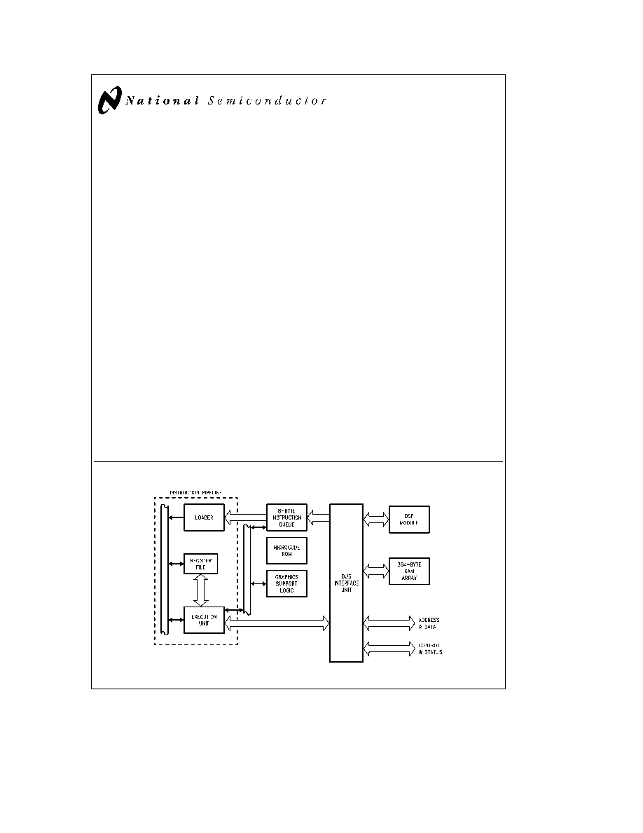
Block Diagram
TL EE 10818 � 67
Series 32000
is a registered trademark of National Semiconductor Corporation
EP
TM
and Embedded System Processors
TM
are trademarks of National Semiconductor Corporation
C1995 National Semiconductor Corporation
RRD-B30M115 Printed in U S A

Table of Contents
1 0 PRODUCT INTRODUCTION
1 1 NS32FX16 Special Features
2 0 ARCHITECTURAL DESCRIPTION
2 1 Register Set
2 1 1 General Purpose Registers
2 1 2 Address Registers
2 1 3 Processor Status Register
2 1 4 Configuration Register
2 1 5 DSP Module Registers
2 1 6 RAM Array
2 2 Memory Organization
2 2 1 Address Mapping
2 3 Modular Software Support
2 4 Instruction Set
2 4 1 General Instruction Format
2 4 2 Addressing Modes
2 4 3 Instruction Set Summary
2 4 Graphic Support
2 5 1 Frame Buffer Addressing
2 5 2 BITBLT Fundamentals
2 5 2 1 Frame Buffer Architecture
2 5 2 2 BIT Alignment
2 5 2 3 Block Boundaries and Destination
Masks
2 5 2 4 BITBLT Directions
2 5 2 5 BITBLT Variations
2 5 3 Graphics Support Instructions
2 5 3 1 BITBLT (BIT-aligned BLock Transfer)
2 5 3 2 Pattern Fill
2 5 3 3 Data Compression Expansion and
Magnify
2 5 3 3 1 Magnifying Compressed Data
3 0 FUNCTIONAL DESCRIPTION
3 1 Instruction Execution
3 1 1 Operating States
3 1 2 Instruction Endings
3 1 2 1 Completed Instructions
3 1 2 2 Suspended Instructions
3 1 2 3 Terminated Instructions
3 1 2 3 Partially Completed Instructions
3 1 3 Slave Processor Instructions
3 1 3 1 Slave Processor Protocol
3 1 3 2 Floating-Point Instructions
3 2 Exception Processing
3 2 1 Exception Acknowledge Sequence
3 2 2 Returning from an Exception Service Procedure
3 2 3 Maskable Interrupts
3 2 3 1 Non-Vectored Mode
3 2 3 2 Vectored Mode Non-Cascaded Case
3 2 3 3 Vectored Mode Cascaded Case
3 2 4 Non-Maskable Interrupt
3 2 5 Traps
3 2 6 Priority among Exceptions
3 2 7 Exception Acknowledge Sequences Detailed
Flow
3 2 7 1 Maskable Non-Maskable Interrupt
Sequence
3 2 7 2 SLAVE ILL SVC DVZ FLG BPT UND
Trap Sequence
3 2 7 3 Trace Trap Sequence
3 3 Debugging Support
3 3 1 Instruction Tracing
3 4 DSP Module (DSPM)
3 4 1 DSPM Operation
3 4 2 Complex Number Representation
3 4 3 DSPM Instructions
3 4 4 Circular Buffers
3 5 System Interface
3 5 1 Power and Grounding
3 5 2 Clocking
3 5 3 Power Save Mode
3 5 4 Resetting
3 5 5 Bus Cycles
3 5 5 1 Bus Status
3 5 5 2 Basic Read and Write Cycles
3 5 5 3 Cycle Extension
3 5 5 4 Instruction Fetch Cycles
3 5 5 5 Interrupt Control Cycles
3 5 5 6 Special Bus Cycles
3 5 5 7 Slave Processor Bus Cycles
3 5 5 8 Data Access Sequences
3 5 5 9 Bus Access Control
3 5 5 10 Instruction Status
2

Table of Contents
(Continued)
4 0 DEVICE SPECIFICATIONS
4 1 NS32FX16 Pin Descriptions
4 1 1 Supplies
4 1 2 Input Signals
4 1 3 Output Signals
4 1 4 Input-Output Signals
4 2 Absolute Maximum Ratings
4 3 Electrical Characteristics
4 4 Switching Characteristics
4 4 1 Definitions
4 4 2 Timing Tables
4 4 2 1 Output Signals Internal Propagation
Delays
4 4 2 2 Input Signal Requirements
4 4 3 Timing Diagrams
Appendix A INSTRUCTION FORMATS
Appendix B INSTRUCTION EXECUTION TIMES
B 1 Basic and Floating-Point Instructions
B 1 1 Equations
B 1 2 Notes on Table Use
B 1 3 Calculation of the Execution Time TEX for Basic
Instructions
B 1 4 Calculation of the Execution Time TEX for
Floating-Point Instructions
B 2 Special Graphics Instructions
B 2 1 Execution Time Calculation for Special
Graphics Instructions
B 3 DSPM Instructions
List of Illustrations
CPU Block Diagram
1-1
NS32FX16 Internal Registers
2-1
Processor Status Register (PSR)
2-2
Configuration Register (CFG)
2-3
DSP Module Registers Address Map
2-4
CPTR Register Format
2-5
CTL Register Format
2-6
ST Register Format
2-7
On-Chip RAM Array Address Map
2-8
NS32FX16 Address Mapping
2-9
NS32FX16 Run-Time Environment
2-10
General Instruction Format
2-11
Index Byte Format
2-12
Displacement Encodings
2-13
Correspondence between Linear and Cartesian Addressing
2-14
32-Pixel by 32-Scan Line Frame Buffer
2-15
Overlapping BITBLT Blocks
2-16
3

List of Illustrations
(Continued)
B B Instructions Format
2-17
BITWT Instruction Format
2-18
EXTBLT Instruction Format
2-19
MOVMPi Instruction Format
2-20
TBITS Instruction Format
2-21
SBITS Instruction Format
2-22
SBITPS Instruction Format
2-23
Bus Activity for a Simple BITBLT Operation
2-24
Operating States
3-1
Slave Processor Protocol
3-2
Slave Processor Status Word
3-3
Interrupt Dispatch Table
3-4
Exception Acknowledge Sequence
3-5
Return from Trap (RETTn) Instruction Flow
3-6
Return from Interrupt (RETI) Instruction Flow
3-7
Interrupt Control Unit Connections (16 Levels)
3-8
Cascaded Interrupt Control Unit Connections
3-9
Exception Processing Flowchart
3-10
Service Sequence
3-11
DSP Module Block Diagram
3-12
Memory Organization of a Complex Vector
3-13
Power and Ground Connections
3-14
Crystal Interconnections
30 MHz
3-15
Crystal Interconnections
40 MHz 50 MHz
3-16
Recommended Reset Connections
3-17
Power-On Reset Requirements
3-18
General Reset Timings
3-19
Bus Connections
3-20
Read Cycle Timing
3-21
Write Cycle Timing
3-22
Cycle Extension of a Read Cycle
3-23
Special Bus Cycle Timing
3-24
Slave Processor Read Cycle
3-25
Slave Processor Write Cycle
3-26
NS32FX16 and FPU Interconnections
3-27
Memory Interface
3-28
HOLD Timing Bus Initially Idle
3-29
HOLD Timing Bus Initially Not Idle
3-30
4

List of Illustrations
(Continued)
Connection Diagram
4-1
Output Signals Specification Standard
4-2
Input Signals Specification Standard
4-3
Read Cycle
4-4
Write Cycle
4-5
Special Bus Cycle
4-6
HOLD Acknowledge Timing (Bus Initially Not Idle)
4-7
HOLD Timing (Bus Initially Idle)
4-8
External DMA Controller Bus Cycle
4-9
Slave Processor Write Timing
4-10
Slave Processor Read Timing
4-11
SPC Timing
4-12
PFS Signal Timing
4-13
ILO Signal Timing
4-14
Clock Waveforms
4-15
INT Signal Timing
4-16
NITI Signal Timing
4-17
Power-On Reset
4-18
Non-Power-On Reset
4-19
List of Tables
NS32FX16 Addressing Modes
2-1
NS32FX16 Instruction Set Summary
2-2
`op' and `i' Field Encodings
2-3
Floating-Point Instruction Protocols
3-1
Summary of Exception Processing
3-2
DSPM Instructions Summary
3-3
Circular Buffer Sizes
3-4
External Oscillator Specifications
3-5
Interrupt Sequences
3-6
Bus Cycle Categories
3-7
Data Access Sequences
3-8
Basic Instructions
B-1
Floating-Point Instructions CPU Portion
B-2
Average Instruction Execution Times with No Wait-States
B-3
Average Instruction Execution Times with Wait-States
B-4
DSPM Instruction Execution Times
B-5
5