
NS486
TM
SXL
Optimized 32-Bit 486-Class Controller with On-Chip
Peripherals for Embedded Systems
General Description
The NS486SXL is a highly integrated embedded system
controller incorporating an Intel486
TM
-class 32-bit processor
along with all of the necessary System Service Elements,
implementing a true "system on a chip." It is ideally suited for
a wide variety of applications running in a segmented
protect-mode environment. The NS486SXL is the second
member of the NS486 family.
Features
n
100% compatible with VxWorks
TM
, VRTX
TM
, QNX
TM
Neutrino, pSOS +
Æ
, and other popular real-time
executives and operating system kernels
n
Intel486 instruction set compatible (protected mode only)
with optimized performance
n
Operation at 25 MHz with 5V supply
n
Low cost 132-pin PQFP package
n
Industry standard interrupt controller, timers, and real
time clock
n
Protected WATCHDOG
TM
timer
n
Optimized DRAM Controller (supports two banks, up to
8 Mbytes each)
n
Up to nine versatile, programmable chip selects
n
Up to eight external interrupts directly supported, and
additional interrupt expansion through an external PIC
interface
n
Glueless interface to ISA-type peripherals
n
Arbitration support for auxiliary processor
n
Support for External Bus Masters, allowing them to
access DRAM and on-chip Peripherals
n
MICROWIRE
TM
/Access.bus synchronous serial
interfaces
n
UART with IrDA v1.0 (Infrared Data Association) port
n
Reconfigurable I/O: Up to 28 I/O pins can be used as
general purpose bidirectional I/O lines
n
Flexible, programmable, multilevel power saving modes
maximize power savings
n
Programming model compatible with the NS486SXF
where possible
Block Diagram NS486SXL Single-Chip Embedded Controller
MICROWIRE
TM
, NS486
TM
and WATCHDOG
TM
are trademarks of National Semiconductor Corporation.
TRI-STATE
Æ
is a registered trademark of National Semiconductor Corporation.
Intel486
TM
is a trademaek of Intel Corporation.
pSOS +
TM
is a trademark of Integrated Systems, Inc.
VRTX
TM
is a registered trademark of Microtec Research, Inc.
PowerPack
Æ
is a registered trademark of Microtek International.
QNX
TM
is a registered trademark of QNX Software Systems, Inc.
VxWorks
TM
is a registered trademark of Wind River Systems, Inc.
DS100121-1
ADVANCE INFORMATION
December 1997
NS486SXL
Optimized
32-Bit
486-Class
Controller
with
On-Chip
Peripherals
for
Embedded
Systems
© 1998 National Semiconductor Corporation
DS100121
www.national.com

Table of Contents
1.0 System Overview
1.1 NS486SXL System Overview
1.2 32-bit Processor Core
1.3 System Service Elements
1.3.1 DRAM Controller
1.3.2 Programmable Interval Timer
1.3.3 WATCHDOG Timer
1.3.4 Interrupt Controller
1.3.5 Real Time Clock/Calendar
1.3.6 Power Management Features
1.4 NS486SXL System Bus
1.5 Other On-board Peripherals
1.5.1 Reconfigurable I/O Lines
1.5.2 MICROWIRE/Access.bus Interface
1.5.3 UART Serial Port
1.6 ICE Support
1.7 Other Issues
2.0 SXL Pin Description Tables
3.0 Device Specifications
3.1 DC Electrical Specifications 5V
±
5%
3.1.1 Recommended Operating Conditions
3.1.2 Absolute Maximum Ratings (Notes 2 and 3)
3.1.3 Capacitance: T
A
= 25∞C, f = 1 MHz
3.1.4 DC Characteristics
3.2 General AC Specifications
3.2.1 Power Ramp Times
3.2.2 PWRGOOD and Power Rampdown Timing
3.3 AC Switching Specifications
3.3.1 DRAM Interface Timing Specification
3.3.2 ISA-like Bus Cycles Timing Specification
3.3.3 Ready Feedback Timing Specifications
3.3.4 OSCX1 AC Specification
4.0 NS486SXL Physical Description
List of Tables
Table 1. Bus Interface Unit Pins
Table 2. External Bus Master Interface Pins
Table 3. DRAM Control Pins
Table 4. Power Pins
Table 5. Reset Logic Pins
Table 6. General Purpose Chip Select Pins
Table 7. Auxiliary Processor Interface Pins
Table 8. Test Pins
Table 9. Interrupt Control Pins
Table 10. Real Time Clock Pins
Table 11. Oscillator Pins
Table 12. 16550 UART Pins
Table 13. Timer Pins
Table 14. 3-Wire Serial I/O Pins
List of Figures
FIGURE 1. NS486SXL Internal Resource to Pins Map
FIGURE 2.NS486SXL Internal Busses
FIGURE 3. NS486SXL Package Pinout Diagram
FIGURE 4. Switching Characteristic Measurement Wave-
forms
FIGURE 5. More Switching Specifications
FIGURE 6. Power Supply Rise and Fall
FIGURE 7. PWGOOD in relation to V
DD
FIGURE 8. DRAM Timing Diagram
FIGURE 9. ISA-like Bus Timing Diagram
FIGURE 10. Ready Feedback Timing Diagram
FIGURE 11.TTL Clock Input Timing Diagram
FIGURE 12. PIC Timing Diagram
FIGURE 13. Access.bus Timing Diagram
FIGURE 14. UART Baud Rate and Infrared Clocks
FIGURE 16. UART MODEM Control Timing
FIGURE 17. NS486SXL Package
www.national.com
2

1.0 System Overview
1.1 NS486SXL SYSTEM OVERVIEW
The NS486SXL is a highly integrated embedded system
controller. It includes an Intel486-class 32-bit processor, all
resources required for the System Service Elements of a
Real-Time Executive, and a selection of key I/O peripherals.
This "system-on-a-chip" is ideal for implementing a wide va-
riety of embedded applications.
The 32-bit processor core executes all of the Intel486 in-
structions with a similar number of clocks per instruction. An
on-board 1 Kbyte instruction cache provides for efficient ex-
ecution from ROM. Intel486 debug features are supported.
The processor has been optimized for operating system ker-
nels such as VRTX, VxWorks, pSOS+ and QNX. These en-
vironments only need the '486 protected mode operation (no
real mode or virtual 8086 support), flat or linear memory ad-
dressing (no virtual memory paging), and floating point ex-
ecution in software only (no co-processor interface).
In fact, the NS486SXL includes all of the System Service El-
ements required by a typical kernel, including an efficient
DRAM controller that supports pagemode DRAMs for data
cache-like performance; three timer channels (including one
configured as a protected WATCHDOG Timer); two pro-
grammable 8259 interrupt controllers provide 15 on-chip in-
terrupt sources; an industry standard real time clock and cal-
endar
(RTC)
with
battery
backup;
and
support
for
comprehensive power management schemes.
In addition, the NS486SXL also incorporates the key I/O pe-
ripherals required for implementing a wide variety of embed-
ded applications: an industry standard high-performance
NS16550-compatible UART with HP-SIR and IrDA v1.0 in-
frared option, an 8254 timer, and a general purpose 2- or
3-wire synchronous serial interface for easy interface to low-
cost EEPROMs and other serial peripherals. System expan-
sion is supported with nine programmable Chip Select (CS)
signals and a generic ISA-type bus interface for external de-
vices and memory.
DS100121-2
***Indicates low-true signals
FIGURE 1. NS486SXL Internal Resource to Pins Map
3
www.national.com

1.0 System Overview
(Continued)
Certain I/O lines not being used by disabled peripherals can
be reconfigured for use as general purpose bidirectional I/O
lines (up to 28 pins). This gives the designer maximum flex-
ibility in designing various systems using the NS486SXL de-
vice. It is expected that an NS486SXL system will minimally
include the NS486SXL system controller with on-board pro-
cessor and I/O devices, boot ROM, and working RAM
memory. Many applications will not require any additional I/O
support.
Finally, the NS486SXL implements a very flexible power
management scheme that permits selective control of indi-
vidual I/O subsystems, with varying levels of power con-
sumption.
NS486SXL provides a cost-effective hardware platform for
the design and implementation of a wide range of internet
appliance, networking and communication systems. With its
powerful embedded '486-class processor, comprehensive
set of on-chip peripheral controllers, flexible power manage-
ment structure and reconfigurable I/O lines, NS486SXL
makes possible a variety of end-user systems based on the
same hardware. Because of its optimized design and on-
board resources, a very cost effective system can be
achieved.
1.2 32-BIT PROCESSOR CORE
The NS486SXL processor core is an implementation of the
protected mode '486 instruction set architecture, optimized
using a RISC-like design philosophy for embedded applica-
tions. Using this approach, the most frequently used instruc-
tions are optimized, and on an average execute in a lower
number of clock cycles than a '486.
The NS486SXL features a three stage pipeline, efficient in-
struction prefetching mechanism, and single cycle instruc-
tion decoding for most instructions. Additionally, a 1 Kbyte in-
struction cache and single cycle DRAM access provide
higher memory performance than a larger unified cache
implementation.
The NS486SXL processor provides the same programming
model and register set as the standard '486 except that real
mode, virtual memory, and floating point support have been
eliminated. These features have little or no impact in embed-
ded applications and save significant silicon real estate. At
reset, unlike the standard '486, the NS486SXL starts up in
protected mode instead of real mode. All '486 instructions
appropriate to protected mode and our hardware configura-
tion are supported, including debug instructions.
The NS486SXL is initially available to run 25 MHz at 5V. The
processor clock is obtained by dividing the crystal frequency
by two. For example, a 25 MHz NS486SXL runs with a
50 MHz crystal oscillator as the master clock.
As a result of our innovative design, the NS486SXL achieves
performance equivalent to a standard '486 with less circuitry.
This translates into reduced power consumption and a lower
overall system cost. It also makes the NS486SXL ideal for
"green" systems and battery operated systems.
1.3 SYSTEM SERVICE ELEMENTS
The NS486SXL controller provides the basic hardware re-
sources required for the O/S-defined System Service Ele-
ments. These include a DRAM controller, programmable in-
terval timer, a protected WATCHDOG timer, a programmable
interrupt controller, a real-time clock and calendar, and com-
prehensive power management features.
1.3.1 DRAM Controller
The NS486SXL DRAM controller supports one or two
adjustable-sized banks of dynamic RAM using a 16-bit data
path. Support is provided for byte parity (if desired), requiring
the DRAM banks to be 18-bits wide when parity is enabled.
Banks can be up to 8 Mbytes in size. The DRAM controller
supports page mode read and write operations and can also
support both byte and word accesses. All access control sig-
nals for read, write and parity checking are generated as well
as an automatic and programmable CAS-before-RAS re-
fresh. If self-refresh DRAMs are used, refresh can be dis-
abled, saving power.
NS486SXL provides flexible support for use of a number of
different DRAM configurations, using popular DRAM de-
vices. Access is optimized for fast page mode DRAMs, and
they will provide the highest performance with contiguous
data. When accessing data bytes or words in the same
DRAM page, the data access is in one cycle. This perfor-
mance provides fast data access times without the overhead
of a separate data cache. Page sizes can be 512, 1024,
2048 or 4096 bytes. Flexibility for DRAM timing is provided
through programming of the DRAM controller registers: 3 or
4 cycle page miss accesses and extended CAS cycles can
be selected.
Memory bank 0 starts at address 0h; memory bank 1 can
start at any address in the 128 Mbyte address map that is a
multiple of its size.
1.3.2 Programmable Interval Timer
The NS486SXL programmable interval timer is compatible
with the Intel 8254 programmable interval timer and contains
three identical timers (CH0≠CH2). CH0 and CH1 can be
used to generate accurate timing delays under software con-
trol. CH2 may be configured to provide a WATCHDOG timer
function.
1.3.3 WATCHDOG Timer
The NS486SXL WATCHDOG timer, CH2, is a protected 16-
bit timer that can be used to prevent system "lockups or
hangups." It uses a 1 kHz clock generated by the on-chip
real-time clock circuit. If the WATCHDOG timer is enabled
and times out, a reset or interrupt will be generated allowing
graceful recovery from an unexpected system lockup.
1.3.4 Interrupt Controller
The NS486SXL interrupt controller consists of two cascaded
programmable interrupt controllers that are compatible with
the Intel 8259A Programmable Interrupt Controller. They pro-
vide a total of 15 (out of 16) programmable interrupts. Three
interrupts are reserved for a real time clock-tick interrupt, a
real time clock interrupt request, and a cascade interrupt
channel. The remaining 13 interrupts can be used by internal
or external sources. Additional external interrupt controllers
can be cascaded as well.
1.3.5 Real Time Clock/Calendar
The NS486SXL Real Time Clock/Calendar is a low power
clock that provides a time-of-day clock and 100-year calen-
dar with alarm features and battery operation. Time is kept in
BCD or binary format. It includes 50 bytes of general pur-
pose CMOS RAM and 3 maskable interrupt sources. It is
compatible with the DS1287 and MC146818 RTC/Calendar
devices, except for the general purpose memory size.
www.national.com
4
1.0 System Overview
(Continued)
1.3.6 Power Management Features
The NS486SXL power management structure includes a
number of power saving mechanisms that can be combined
to achieve comprehensive power savings under a variety of
system conditions. First of all, the core processor power con-
sumption can be controlled by varying the processor/system
clock frequency. The internal CPU clock can be divided by 4,
8, 16, 32 or 64. In addition, in idle mode, the internal proces-
sor clock will be disabled. Finally, if an external crystal oscil-
lator circuit is being used, it can be disabled. For maximum
power savings, all internal clocks can be disabled (except for
the real-time clock oscillator).
The clocks of the on-board peripherals can be individually or
globally controlled. By setting bits in the power management
control registers, the internal clocks to the three-wire inter-
face, the timer, the DRAM controller, and the UART can be
disabled.
In addition to these internal clocks, the external SYSCLK can
be disabled via a bit in the power management control regis-
ters.
Using various combinations of these power saving controls
with the NS486SXL controller will result in excellent pro-
grammable power management for any application.
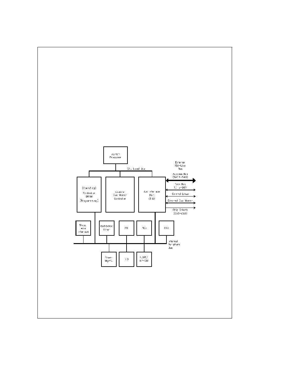
1.4 NS486SXL SYSTEM BUS
The NS486SXL system bus provides the interface to off-chip
peripherals and memory. It offers an ISA compatible inter-
face and is therefore capable of directly interfacing to many
ISA peripheral control devices. The interface is accom-
plished through the Bus Interface Unit (BIU). The BIU gener-
ates all of the access signals for both internal and external
peripherals and memory. Depending upon whether the ac-
cess is to internal peripherals, external peripherals or exter-
nal memory, the BIU generates the timing and control sig-
nals to access those resources. The BIU is designed to
support a glueless interface to many ISA-type peripherals.
For debug purposes, the NS486SXL can be set to generate
external bus cycles at the same time as an internal periph-
eral access takes place. This gives logic analyzers or other
debug tools the ability to track and capture internal periph-
eral accesses.
Access to internal peripherals is accomplished in three CPU
T-states (clock cycles). The fastest access to off-chip I/O is
also three T-states. When accessing off-chip memory and
I/O, wait state generation is accomplished through a combi-
nation of NS486SXL chip select logic and off-chip peripheral
feedback signals.
The ISA-like bus on the NS486SXL also supports External
Bus Masters. This feature allows external processors or I/O
Peripherals (and customer proprietary ASICs) with built-in
DMA controllers to read and write System DRAM supported
by the 'SXL DRAM Controller. External Masters can also ac-
cess any internal or external peripherals or memory as well.
The external master address must be at TRI-STATE
Æ
(through external address transceivers if necessary) in order
to support external master access to the DRAM.
DS100121-3
FIGURE 2. NS486SXL Internal Busses
5
www.national.com