 | –≠–ª–µ–∫—Ç—Ä–æ–Ω–Ω—ã–π –∫–æ–º–ø–æ–Ω–µ–Ω—Ç: R76201BEA | –°–∫–∞—á–∞—Ç—å:  PDF PDF  ZIP ZIP |
54AC151/54ACT151
8-Input Multiplexer
General Description
The 'AC/'ACT151 is a high-speed 8-input digital multiplexer.
It provides, in one package, the ability to select one line of
data from up to eight sources. The 'AC/'ACT151 can be used
as a universal function generator to generate any logic func-
tion of four variables. Both true and complementary outputs
are provided.
Features
n
I
CC
reduced by 50%
n
Outputs source/sink 24 mA
n
'ACT151 has TTL-compatible inputs
n
Standard Microcircuit Drawing (SMD)
-- 'AC151: 5962-87691
-- 'ACT151: 5962-88756
n
54AC151 now qualified to 300Krad RHA designation,
refer to the SMD for more information
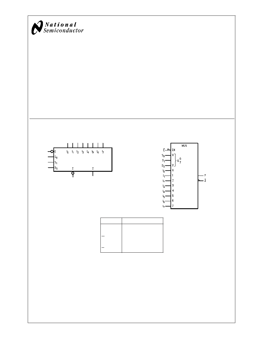
Logic Symbols
IEEE/IEC
10027001
10027006
Pin Names
Description
I
0
≠I
7
Data Inputs
S
0
≠S
2
Select Inputs
E
Enable Input
Z
Data Output
Z
Inverted Data Output
FACT
Æ
is a registered trademark of Fairchild Semiconductor Corporation.
July 2003
54AC151/54ACT151
8-Input
Multiplexer
© 2003 National Semiconductor Corporation
DS100270
www.national.com
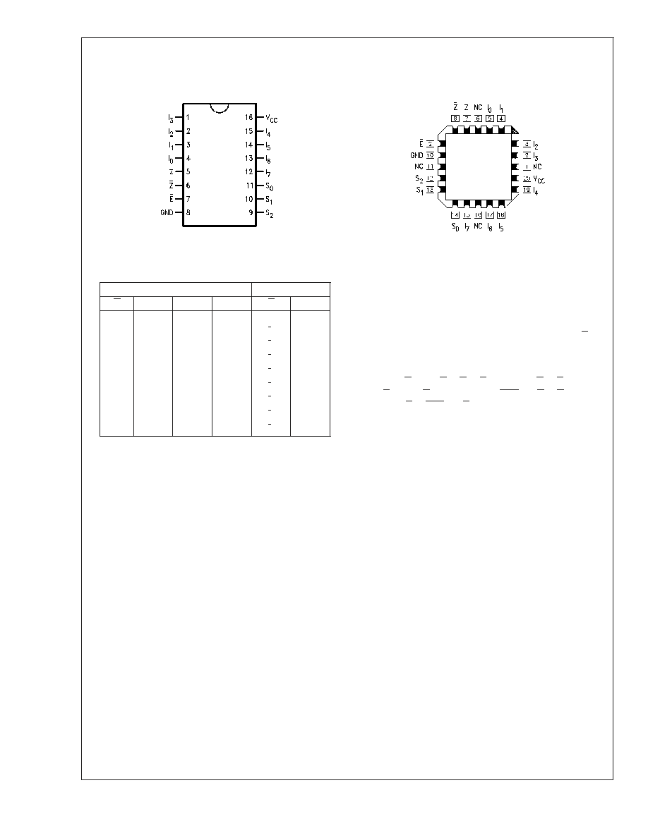
Connection Diagrams
Pin Assignment
for DIP and Flatpak
Pin Assignment
for LCC
10027002
10027003
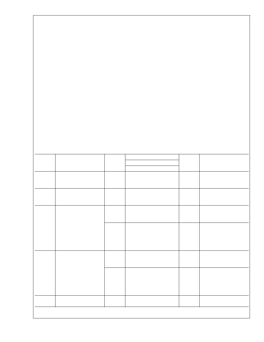
Truth Table
Inputs
Outputs
E
S
2
S
1
S
0
Z
Z
H
X
X
X
H
L
L
L
L
L
I
0
I
0
L
L
L
H
I
1
I
1
L
L
H
L
I
2
I
2
L
L
H
H
I
3
I
3
L
H
L
L
I
4
I
4
L
H
L
H
I
5
I
5
L
H
H
L
I
6
I
6
L
H
H
H
I
7
I
7
H = HIGH Voltage Level
L = LOW Voltage Level
X = Immaterial
Functional Description
The 'AC/'ACT151 is a logic implementation of a single pole,
8-position switch with the switch position controlled by the
state of three Select inputs, S
0
, S
1
, S
2
. Both true and
complementary outputs are provided. The Enable input (E) is
active LOW. When it is not activated, the complementary
output is HIGH and the true output is LOW regardless of all
other inputs. The logic function provided at the output is:
Z = E
∑
(I
0
∑
S
0
∑
S
1
∑
S
2
+ I
1
∑
S
0
∑
S
1
∑
S
2
+
I
2
∑
S
0
∑
S
1
∑
S
2
+ I
3
∑
S
0
∑
S
1
∑
S
2
+ I
4
∑
S
0
∑
S
1
∑
S
2
+
I
5
∑
S
0
∑
S
1
∑
S
2
+ I
6
∑
S
0
∑
S
1
∑
S
2
+ I
7
∑
S
0
∑
S
1
∑
S
2
)
The 'AC/'ACT151 provides the ability, in one package to
select from eight sources of data or control information. By
proper manipulation of the inputs, the 'AC/'ACT151 can
provide any logic function of four variables and its comple-
ment.
54AC151/54ACT151
www.national.com
2
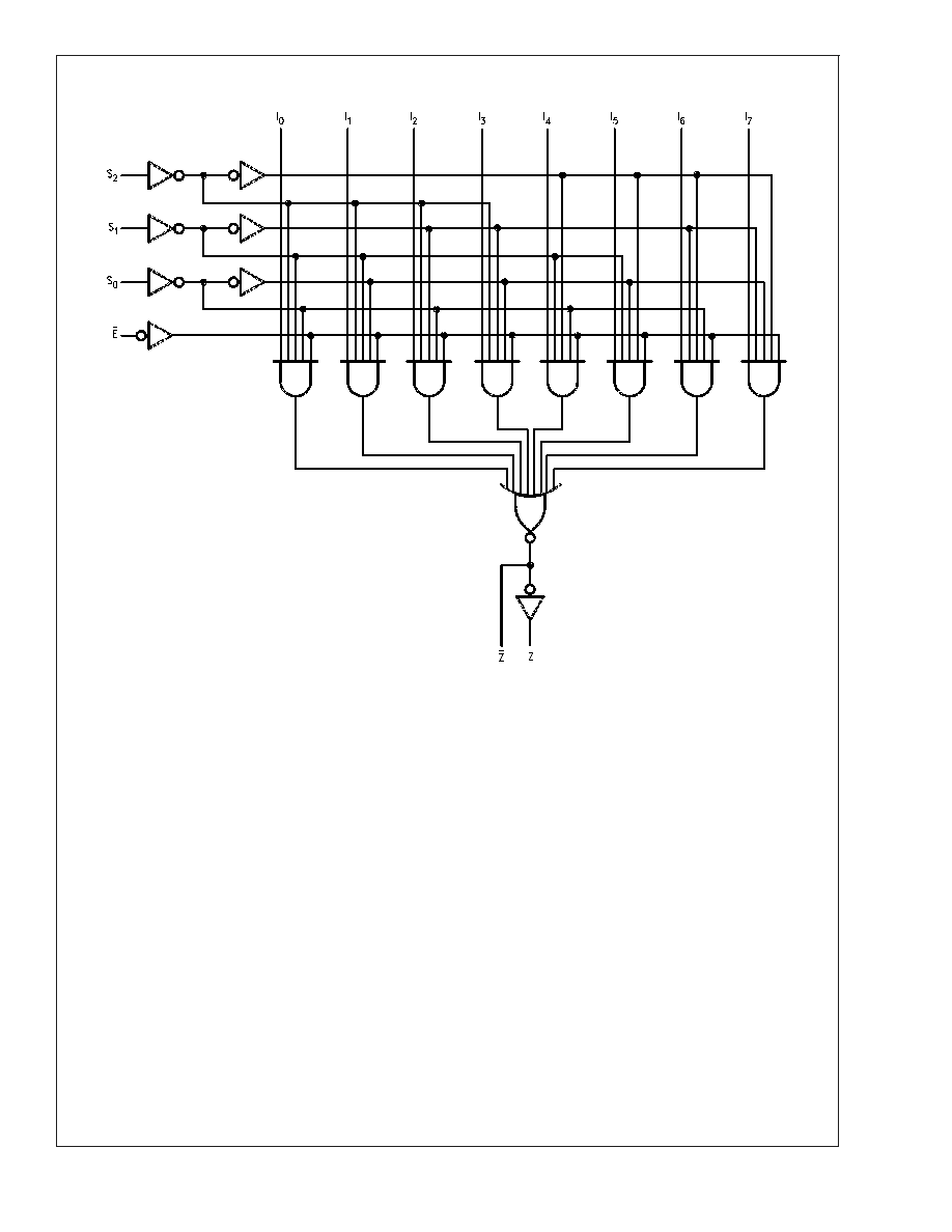
Logic Diagram
10027004
Please note that this diagram is provided only for the understanding of logic operations and should not be used to estimate propagation delays.
54AC151/54ACT151
www.national.com
3
Absolute Maximum Ratings
(Note 1)
If Military/Aerospace specified devices are required,
please contact the National Semiconductor Sales Office/
Distributors for availability and specifications.
Supply Voltage (V
CC
)
-0.5V to +7.0V
DC Input Diode Current (I
IK
)
V
I
= -0.5V
-20 mA
V
I
= V
CC
+ 0.5V
+20 mA
DC Input Voltage (V
I
)
-0.5V to V
CC
+
0.5V
DC Output Diode Current (I
OK
)
V
O
= -0.5V
-20 mA
V
O
= V
CC
+ 0.5V
+20 mA
DC Output Voltage (V
O
)
-0.5V to V
CC
+
0.5V
DC Output Source
or Sink Current (I
O
)
±
50 mA
DC V
CC
or Ground Current
per Output Pin (I
CC
or I
GND
)
±
50 mA
Storage Temperature (T
STG
)
-65∞C to +150∞C
Junction Temperature (T
J
)
CDIP
175∞C
Recommended Operating
Conditions
Supply Voltage (V
CC
)
'AC
2.0V to 6.0V
'ACT
4.5V to 5.5V
Input Voltage (V
I
)
0V to V
CC
Output Voltage (V
O
)
0V to V
CC
Operating Temperature (T
A
)
54AC/ACT
-55∞C to +125∞C
Minimum Input Edge Rate (
V/t)
'AC Devices
V
IN
from 30% to 70% of V
CC
V
CC
@
3.3V, 4.5V, 5.5V
125 mV/ns
Minimum Input Edge Rate (
V/t)
'ACT Devices
V
IN
from 0.8V to 2.0V
V
CC
@
4.5V, 5.5V
125 mV/ns
Note 1: Absolute maximum ratings are those values beyond which damage
to the device may occur. The databook specifications should be met, without
exception, to ensure that the system design is reliable over its power supply,
temperature, and output/input loading variables. National does not recom-
mend operation of FACT
Æ
circuits outside databook specifications.
DC Characteristics for 'AC Family Devices
54AC
Symbol
Parameter
V
CC
T
A
= -55∞C to +125∞C
Units
Conditions
(V)
Guaranteed Limits
V
IH
Minimum High Level
3.0
2.1
V
OUT
= 0.1V
Input Voltage
4.5
3.15
V
or V
CC
- 0.1V
5.5
3.85
V
IL
Maximum Low Level
3.0
0.9
V
OUT
= 0.1V
Input Voltage
4.5
1.35
V
or V
CC
- 0.1V
5.5
1.65
V
OH
Minimum High Level
3.0
2.9
I
OUT
= -50 µA
Output Voltage
4.5
4.4
V
5.5
5.4
(Note 2)
V
IN
= V
IL
or V
IH
3.0
2.4
I
OH
= -12 mA
4.5
3.7
V
I
OH
= -24 mA
5.5
4.7
I
OH
= -24 mA
V
OL
Maximum Low Level
3.0
0.1
I
OUT
= 50 µA
Output Voltage
4.5
0.1
V
5.5
0.1
(Note 2)
V
IN
= V
IL
or V
IH
3.0
0.50
I
OL
= 12 mA
4.5
0.50
V
I
OL
= 24 mA
5.5
0.50
I
OL
= 24 mA
I
IN
Maximum Input
5.5
±
1.0
µA
V
I
= V
CC
, GND
Leakage Current
54AC151/54ACT151
www.national.com
4
DC Characteristics for 'AC Family Devices
(Continued)
54AC
Symbol
Parameter
V
CC
T
A
= -55∞C to +125∞C
Units
Conditions
(V)
Guaranteed Limits
I
OLD
Minimum Dynamic
Output Current (Note 3)
5.5
50
mA
V
OLD
= 1.65V Max
I
OHD
5.5
-50
mA
V
OHD
= 3.85V Min
I
CC
Maximum Quiescent
5.5
80.0
µA
V
IN
= V
CC
Supply Current
or GND
Note 2: All outputs loaded; thresholds on input associated with output under test.
Note 3: Maximum test duration 2.0 ms, one output loaded at a time.
Note 4: I
IN
and I
CC
@ 3.0V are guaranteed to be less than or equal to the respective limit @ 5.5V V
CC
.
I
CC
for 54AC @ 25∞C is identical to 74AC @ 25∞C
DC Characteristics for 'ACT Family Devices
54ACT
Symbol
Parameter
V
CC
T
A
= -55∞C to +125∞C
Units
Conditions
(V)
Guaranteed Limits
V
IH
Minimum High Level
4.5
2.0
V
V
OUT
= 0.1V
Input Voltage
5.5
2.0
or V
CC
- 0.1V
V
IL
Maximum Low Level
4.5
0.8
V
V
OUT
= 0.1V
Input Voltage
5.5
0.8
or V
CC
- 0.1V
V
OH
Minimum High Level
4.5
4.4
V
I
OUT
= -50 µA
Output Voltage
5.5
5.4
(Note 5)
V
IN
= V
IL
or V
IH
4.5
3.70
V
I
OH
= -24 mA
5.5
4.70
I
OH
= -24 mA
V
OL
Maximum Low Level
4.5
0.1
V
I
OUT
= 50 µA
Output Voltage
5.5
0.1
(Note 5)
V
IN
= V
IL
or V
IH
4.5
0.50
V
I
OL
= 24 mA
5.5
0.50
I
OL
= 24 mA
I
IN
Maximum Input
5.5
±
1.0
µA
V
I
= V
CC
, GND
Leakage Current
I
CCT
Maximum
5.5
1.6
mA
V
I
= V
CC
- 2.1V
I
CC
/Input
I
OLD
Minimum Dynamic
5.5
50
mA
V
OLD
= 1.65V Max
I
OHD
Output Current (Note 6)
5.5
-50
mA
V
OHD
= 3.85V Min
I
CC
Maximum Quiescent
5.5
80.0
µA
V
IN
= V
CC
Supply Current
or GND
Note 5: All outputs loaded; thresholds on input associated with output under test.
Note 6: Maximum test duration 2.0 ms, one output loaded at a time.
Note 7: I
CC
for 54ACT @ 25∞C is identical to 74ACT @ 25∞C.
54AC151/54ACT151
www.national.com
5