
U
S
B
N
9
6
0
2
(
U
n
i
v
e
r
s
a
l
S
e
r
i
a
l
B
u
s
)
F
u
l
l
S
p
e
e
d
F
u
n
c
t
i
o
n
C
o
n
t
r
o
l
l
e
r
W
i
t
h
D
M
A
S
u
p
p
o
r
t
�
1998 National Semiconductor Corporation
www.national.com
November 1998
USBN9602 (Universal Serial Bus)
Full Speed Function Controller With DMA Support
1.0 General Description
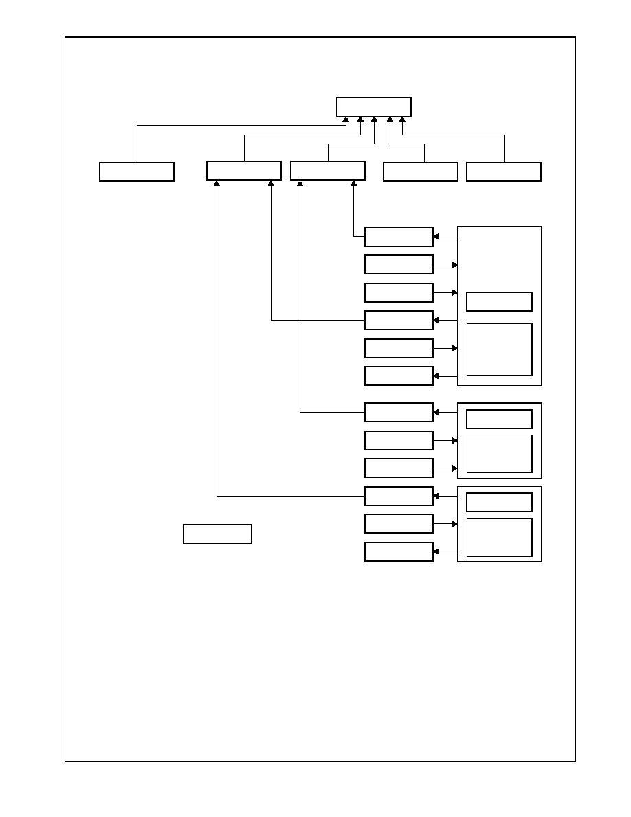
The USBN9602 is an integrated USB Node controller com-
patible with the USB Specification Versions 1.0 and 1.1.
Integrated onto a single IC are the required USB trans-
ceiver with a 3.3V Regulator, Media Access Controller,
USB endpoint (EP) FIFOs, a versatile 8-bit parallel inter-
face, MICROWIRE/PLUSTM Interface and a clock genera-
tor. A total of seven FIFO buffers support the different USB
messages: one bidirectional FIFO for the mandatory con-
Block Diagram
TRI-STATE
�
is a registered trademark of National Semiconductor Corporation.
MICROWIRE/PLUS
TM
and MICROWIRE
TM
are trademarks of National Semiconductor Corporation.
Physical Layer Interface (PHY)
Media Access Controller (MAC)
Transceiver
48 MHz
Oscillator
Clock
Generator
XIN
XOUT
CLKOUT
Microcontroller Interface
D+
D-
Upstream Port
INTR
V3.3
CS
RD
WR
A0/ALE
D[7:0]/AD[7:0]
E
P
2
E
n
d
p
o
i
n
t
0
E
P
1
E
P
6
E
P
5
RX
TX
Endpoint/Control FIFOs
VReg
AGND
RESET
Vcc
GND
MODE[1:0]
Status
Control
SIE
USB Event
Detect
Clock
Recovery
E
P
4
E
P
3
trol endpoint EP0 and six FIFOs for an additional six unidi-
rectional Endpoint Pipes to support USB interrupt, bulk and
isochronous data transfers. The 8-bit parallel interface sup-
ports multiplexed and non-multiplexed style CPU
address/data buses. A programmable interrupt output
scheme allows device configuration for different interrupt
signaling requirements.

2
www.national.com
2.0 Features
s
Full-Speed USB Node Device
s
USB transceiver
s
3.3V signal voltage regulator
s
48 MHz oscillator circuit
s
Programmable clock generator
s
Serial Interface Engine consisting of Physical Layer In-
terface (PHY) and Media Access Controller (MAC), USB
Specification 1.0 compliant
s
Control/Status Register File
s
USB Function Controller with seven FIFO-based End-
points:
� One bidirectional Control Endpoint 0 (8 bytes)
� Three Transmit Endpoints (2*32 and 1*64 bytes)
� Three Receive Endpoints (2*32 and 1*64 bytes)
s
8-bit parallel interface with two selectable modes:
� non-multiplexed
� multiplexed (Intel compatible)
s
DMA support for parallel interface
s
MICROWIRE/PLUSTM Interface
s
28-pin SO package

3
www.national.com
Table of Contents
1.0
General Description . . . . . . . . . . . . . . . . . . . . . . . . . . . . 1
2.0
Features . . . . . . . . . . . . . . . . . . . . . . . . . . . . . . . . . . . . . . 2
3.0
Device Overview . . . . . . . . . . . . . . . . . . . . . . . . . . . . . . . 4
3.1
Transceiver . . . . . . . . . . . . . . . . . . . . . . . . . . . . . . 4
3.2
Voltage Regulator (VReg) . . . . . . . . . . . . . . . . . . . 4
3.3
Serial Interface Engine (SIE) . . . . . . . . . . . . . . . . . 4
3.4
Endpoint/Control FIFOs . . . . . . . . . . . . . . . . . . . . . 4
3.5
Microcontroller Interface . . . . . . . . . . . . . . . . . . . . 5
4.0
Connection Diagram . . . . . . . . . . . . . . . . . . . . . . . . . . . 5
5.0
Pin Descriptions . . . . . . . . . . . . . . . . . . . . . . . . . . . . . . . 6
6.0
Parallel Interface . . . . . . . . . . . . . . . . . . . . . . . . . . . . . . . 9
6.1
Non-Multiplexed Mode . . . . . . . . . . . . . . . . . . . . . . 9
6.2
Multiplexed Mode . . . . . . . . . . . . . . . . . . . . . . . . . 10
7.0
DMA Support . . . . . . . . . . . . . . . . . . . . . . . . . . . . . . . . . 12
8.0
MICROWIRE/PLUS Interface . . . . . . . . . . . . . . . . . . . . 13
9.0
Device Functional States . . . . . . . . . . . . . . . . . . . . . . . 16
9.1
Suspend Operation . . . . . . . . . . . . . . . . . . . . . . . 16
9.2
Remote Resume . . . . . . . . . . . . . . . . . . . . . . . . . 16
9.3
USB Resume Operation . . . . . . . . . . . . . . . . . . . 16
9.4
Functional State Transitions . . . . . . . . . . . . . . . . 16
10.0
Endpoint Operation . . . . . . . . . . . . . . . . . . . . . . . . . . . 18
10.1
Transmit and Receive Endpoint FIFOs . . . . . . . . 18
10.2
Bidirectional Control Endpoint FIFO0 Operation . 19
10.3
Transmit Endpoint FIFO Operation (TXFIFO1,
TXFIFO2, TXFIFO3) . . . . . . . . . . . . . . . . . . . . . . 19
10.4
Receive Endpoint FIFO Operation (RXFIFO1,
RXFIFO2, RXFIFO3) . . . . . . . . . . . . . . . . . . . . . . 20
10.5
Programming Model . . . . . . . . . . . . . . . . . . . . . . 21
11.0
Register Set . . . . . . . . . . . . . . . . . . . . . . . . . . . . . . . . . . 23
11.1
Main Control Register (MCNTRL) . . . . . . . . . . . . 23
11.2
Clock Configuration Register (CCONF) . . . . . . . . 23
11.3
DMA Control Register (DMACNTRL) . . . . . . . . . 24
11.4
Revision Identifier Register (RID)Revision Identifier (RID)
24
11.5
Node Functional State Register (NFSR) . . . . . . . 24
11.6
Main Event Register (MAEV) . . . . . . . . . . . . . . . . 25
11.7
Main Mask Register (MAMSK) . . . . . . . . . . . . . . 25
11.8
Alternate Event Register (ALTEV) . . . . . . . . . . . . 25
11.9
Alternate Mask Register (ALTMSK) . . . . . . . . . . . 26
11.10 Transmit Event Register (TXEV) . . . . . . . . . . . . . 26
11.11 Transmit Mask Register (TXMSK) . . . . . . . . . . . 26
11.12 Receive Event Register (RXEV) . . . . . . . . . . . . . 27
11.13 Receive Mask Register (RXMSK) . . . . . . . . . . . 27
11.14 NAK Event Register (NAKEV) . . . . . . . . . . . . . . 27
11.15 NAK Mask Register (NAKMSK) . . . . . . . . . . . . . 27
11.16 FIFO Warning Event Register (FWEV) . . . . . . . . 27
11.17 FIFO Warning Mask Register (FWMSK) . . . . . . 28
11.18 Frame Number High Byte Register (FNH) . . . . . 28
11.19 Frame Number Low Byte Register (FNL) . . . . . . 28
11.20 Function Address Register (FAR) . . . . . . . . . . . . 28
11.21 Endpoint Control Register 0 (EPC0) . . . . . . . . . . 29
11.22 Transmit Status Register 0 (TXS0) . . . . . . . . . . . 29
11.23 Transmit Command Register 0 (TXC0) . . . . . . . 29
11.24 Transmit Data Register 0 (TXD0) . . . . . . . . . . . . 30
11.25 Receive Status Register 0 (RXS0) . . . . . . . . . . . 30
11.26 Receive Command Register 0 (RXC0) . . . . . . . . 30
11.27 Receive Data Register 0 (RXD0) . . . . . . . . . . . . 31
11.28 Endpoint Control Register x (EPC1 through
EPC6) . . . . . . . . . . . . . . . . . . . . . . . . . . . . . . . . . 31
11.29 Transmit Status Register x (TXS1, TXS2, TXS3) 31
11.30 Transmit Command Register x (TXC1, TXC2, TXC3)
32
11.31 Transmit Data Register x (TXD1, TXD2, TXD3) . 32
11.32 Receive Status Register x (RXS1, RXS2, RXS3) 33
11.33 Receive Command Register x (RXC1, RXC2, RXC3)
33
11.34 Receive Data Register x (RXD1, RXD2, RXD3) . 34
12.0
Design considerations . . . . . . . . . . . . . . . . . . . . . . . . 35
12.1
Targeted Applications . . . . . . . . . . . . . . . . . . . . . 35
12.2
3.3V Regulator Issues . . . . . . . . . . . . . . . . . . . . 35
12.3
Simplified Application Diagrams . . . . . . . . . . . . . 35
13.0
Memory Map . . . . . . . . . . . . . . . . . . . . . . . . . . . . . . . . 36
14.0
Electrical Characteristics - PRELIMINARY . . . . . . . . 37
14.1
Parallel Interface Timing (MODE[1:0] = 00b) . . . 39
14.2
Parallel Interface Timing (MODE[1:0] = 01b) . . . 41
14.3
DMA Support Timing . . . . . . . . . . . . . . . . . . . . . 43
14.4
MICROWIRE Interface Timing
(MODE[1:0] = 10b) . . . . . . . . . . . . . . . . . . . . . . . 44
15.0
Physical Dimensions . . . . . . . . . . . . . . . . . . . . . . . . . 45

4
www.national.com
3.0 Device Overview
The USBN9602 is an integrated USB Node controller. The
block diagram on page 1 of the data sheet shows the ma-
jor on-chip components of the device.
3.1 Transceiver
The USBN9602 contains a high-speed transceiver, which
consists of three main functional blocks:
� differential receiver
� single-ended receiver with on-chip voltage reference
� transmitter with on-chip current source
The performance requirements met by this transceiver are
described in Chapter 7 of the Universal Serial Bus Speci-
fication Version 1.0.
To minimize signal skew, the differential output swings of
the transmitter are well balanced. Slew-rate control is
used on the driver to minimize radiated noise and cross
talk. The drivers support TRI-STATE� operation to allow
bidirectional half-duplex operation of the transceiver.
The differential receiver operates over the complete com-
mon mode range, that is guaranteed to be larger than that
of the single-ended receivers, to avoid potential glitches in
the Serial Interface Engine (SIE) after Single-Ended Ze-
ros.
Single-ended receivers are present on each of the two
data lines. These are required, in addition to the differen-
tial receiver, to detect an absolute voltage with a switching
threshold between 0.8V and 2.0V (TTL inputs). An exter-
nal 1.5
�
5% k
resistor, tied to a voltage source between
3.0V and 3.6V referenced to the local ground, is required
on D+ to indicate that this is a high-speed node.
3.2 Voltage Regulator (VReg)
The Voltage Regulator provides a 3.3V voltage from the
5.0V device power for the integrated transceiver. This
3.3V output can be used to supply power to the 1.5 k
pull-up resistor. It can be disabled under software control
to allow using the device in a 3.3V system. This output
must be decoupled with a 10
�
F tantalum capacitor to
ground.
3.3 Serial Interface Engine (SIE)
The USB Serial Interface Engine (SIE) consists of a Phys-
ical Layer Interface (PHY) level and a Media Access Con-
troller (MAC) level. The PHY level includes the digital-
clock recovery circuit, a digital glitch filter, End_Of_Packet
detection circuitry, and bit stuffing and unstuffing logic.
The MAC level includes packet formatting, CRC genera-
tion and checking, endpoint address detection, and pro-
vides the necessary control to give the NAK, ACK, and
STALL responses as determined by the Endpoint Control-
ler for the specified endpoint pipe. The SIE is also respon-
sible for detecting and reporting events on detection of
USB-specific events such as Reset, Suspend, and Re-
sume. The transmitter outputs of the module to the trans-
ceiver are well matched (under 1 ns) to minimize skew on
the USB signals.
The USB standard specifies bit stuffing and unstuffing as
a method to ensure adequate transitions on the line to en-
able clock recovery at the receiving end. Whenever a
string of consecutive 1s is encountered, the bit-stuffing
logic inserts a 0 after every sixth 1 in the data stream. The
bit-unstuffing logic reverses this process.
The clock recovery block uses the incoming NRZI data to
extract a data clock (12 MHz) from an input clock derived
from a crystal or crystal oscillator (48 MHz frequency).
This clock is used in the data recovery circuit. The output
of this block is binary data (decoded from the NRZI
stream) that can be appropriately sampled using the ex-
tracted 12 MHz clock. The jitter performance and timing
characteristics meet the requirements set forth in Chapter
7 of the USB Specification.
3.4 Endpoint/Control FIFOs
The Endpoint Pipe Controller (EPC) provides the interface
for USB Function endpoints. An endpoint is the ultimate
source or sink of data. An endpoint pipe provides for the
movement of data between USB and memory, and com-
pletes the path between the USB Host and the function
endpoint. According to the USB specification, up to 31
such endpoint pipes are supported at any given time,
each with the same Function Address. The USBN9602,
however, supports a maximum of seven endpoint pipes.
A USB Function is a USB device that is able to transmit
and receive information on the bus. A Function may have
one or more configurations, each of which defines the in-
terfaces that make up the device. Each interface, in turn,
is composed of one or more endpoints.
Each endpoint is an addressable entity on USB and is re-
quired to respond to IN and OUT tokens from the USB
Host (typically a PC). An IN token indicates that the host
has requested to receive information from an endpoint,
and an OUT token indicates that the host is about to send
information to an endpoint.
Upon detection of an IN token addressed to an endpoint,
the endpoint is responsible for responding with a data
packet. If the endpoint is currently stalled, a STALL hand-
shake packet is sent under software control. If the end-
point is enabled, but no data is present, a NAK (Negative
Acknowledgment) handshake packet is sent automatically.
If the Endpoint is Isochronous and enabled, but no data
present, a bit stuff error followed by an end of packet is
sent on the bus.
Similarly, upon detection of an OUT token addressed to
an endpoint, the endpoint is responsible for receiving a
data packet sent by the host and storing it in a buffer. If
the endpoint pipe is currently stalled, a STALL handshake
packet is sent at the end of the data transmission. If the
endpoint pipe is currently disabled, no handshake packet
is sent at the end of the data transmission. If the endpoint
pipe is enabled, but no buffer is present in which to store
the data, a NAK (Negative Acknowledgment) handshake
packet is sent. If the Endpoint is Isochronous and enabled
but can't handle the data, the data will be lost.
5
www.national.com
A Disabled endpoint does not respond to IN, OUT, or
SETUP tokens.
The Endpoint Pipe Controller maintains separate status
and control information for each endpoint pipe.
For IN tokens, the Endpoint Pipe Controller is responsible
for transferring data from the defined buffer to the host.
For OUT tokens, the Endpoint Pipe Controller is responsi-
ble for transferring data from the host to the defined buffer.
3.5 Microcontroller Interface
A CPU or microcontroller can be connected via an 8-bit
parallel interface or a MICROWIRE interface. For the par-
allel interface, there are two addressing modes (multi-
plexed or non-multiplexed). These modes are selected by
hardwiring the proper binary code on the MODE1 and
MODE0 pins.
In addition, an interrupt output is provided. The type of the
interrupt can be programmed to be either push-pull active-
high or active-low output, or an open-drain active-low out-
put.
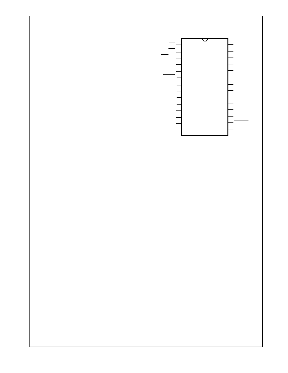
4.0 Connection Diagram
Figure 1. USBN9602 Connection Diagram
CS
RD
WR/SK
DACK
GND
Vcc
GND
MODE1
MODE0
D6
D5
D4
D3
1
2
3
4
5
6
7
8
9
10
11
12
13
14
28
27
26
25
24
23
22
21
20
19
18
17
16
15
INTR
XOUT
XIN
CLKOUT
D7
AGND
D�
D+
V3.3
RESET
A0/ALE/SI
D0/SO
D1
D2
28 pin
SO
DRQ
Order Number USBN9602-28M
See NS Package Number M28B
6
www.national.com
5.0 Pin Descriptions
The following tables briefly describe the USBN9602 pins.
Each table lists a related set of device pins and shows the
device pin number, the signal direction ("I" for input, "O"
for output, "I/O" for bidirectional, or N.A. for not applica-
ble), and a brief description of the pin function.
Note that unused input or bidirectional pins must be pulled
up or down as appropriate. This is essential to reduce
overall power consumption and to limit EMI.
5.0.1 Power Supply
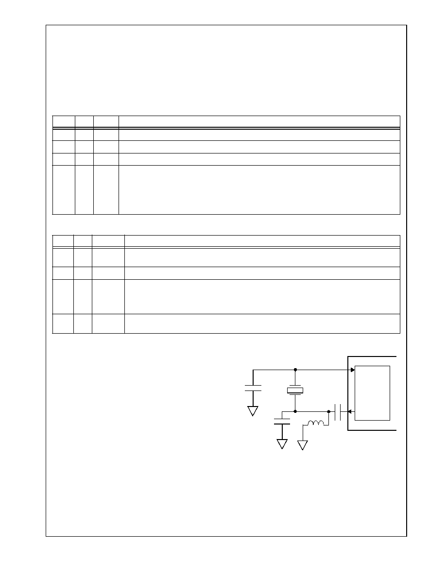
5.0.2 Oscillator, Clock and Reset
Oscillator Circuits
The XIN and XOUT pins may be connected to make a 48
MHz closed loop crystal controlled oscillator. Alternately an
external 48 MHz clock source may be input to clock the
device. The internal crystal oscillator uses a 48 MHz 3rd
harmonic crystal. The circuit for the crystal option is shown
in Figure 2. If an external clock source is used, it is con-
nected to XIN. XOUT is unconnected.
Stray capacitance and inductance should be kept as low as
possible in the oscillator circuit. Trace lengths should be
minimized by locating the crystal and external components
as close as possible to the XIN and XOUT pins.
Note: The circuit shown has been tested with crystals from
ECS Inc. only (e.g. part number ECS-480-S-1-3OT). For
other crystals , please consult the manufacturer for recom-
mended circuit and component values.
Pin #
Dir
Label
Pin Functional Description
22
N.A. Vcc
Digital Power Supply (Vcc)
21,23
N.A. GND
Digital Power Supply (GND)
17
N.A. AGND
Analog Power Supply (AGND)
18
N.A. V3.3
Transceiver 3.3V Voltage Supply. This pin can be used as the internal 3.3V voltage regulator out-
put. The regulator is intended to power only the internal transceiver and one external pull-up. An
external
1
�
F
de-coupling capacitor is required on this pin. The voltage regulator output is dis-
abled upon hardware reset. If the internal voltage regulator is left disabled, this pin can be used
as an 3.3V supply input for the transceiver.
Pin #
Dir
Label
Pin Functional Description
26
N.A. XIN
Input for internal 48 MHz crystal oscillator circuit. A 48 MHz third harmonic crystal may be used.
27
N.A. XOUT
Output for the internal crystal oscillator circuit.
28
O
CLKOUT
Clock Output. This pin provides a programmable clock source. Upon hardware reset, this pin
sources a 4 MHz clock (there may be an initial phase discontinuity). It may be programmed for
different speeds or disabled via the Clock Configuration Register (these subsequent transitions
are synchronous and will occur smoothly).
16
I
RESET
Active-Low Reset input. Signal conditioning is provided on this pin to allow the use of a simple
RC power-on reset circuit.
Figure 2. 3rd Harmonic Crystal Oscillator
Connections
XTAL1
C2
C1
48 MHz
OSC
XIN
C3
L1

7
www.national.com
5.0 Pin Descriptions
(Continued)
5.0.3 USB Port
Component
Parameters
Values
Tolerance
Crystal 1
Resonance Frequency
Third Overtone
Type
Maximum Effective Series Resistance
Maximum Shunt Capacitance
Maximum Drive Level
48 MHz
Parallel
AT-Cut
40
7 pF
1 mW
2500 ppm
C1
22 pF
10%
C2
56 pF
10%
C3
100 nF
10%
L1
470 nH
10%
Pin #
Dir
Label
Pin Functional Description
19
I/O
D+
USB D+ upstream port. This pin requires an external 1.5k pull-up to 3.3V to signal full speed
operation.
20
I/O
D�
USB D� upstream port.

5.0 Pin Descriptions
(Continued)
8
www.national.com
5.0.4 Microprocessor Interface
Pin #
Dir
Label
Pin Functional Description
24:25
I
MODE[1:0] Interface Mode select input pins. Each of these pins should be hard-wired to Vcc or GND
to select the interface mode:
MODE[1:0] = 00: Mode 0: non-multiplexed parallel interface mode
MODE[1:0] = 01: Mode 1: multiplexed parallel interface mode
MODE[1:0] = 10: Mode 2: MICROWIRE interface mode
MODE[1:0] = 11: Mode 3: reserved
Note: Mode 3 also selects the MICROWIRE interface mode in the USBN9602, but this
mode should be reserved to preserve compatibility with future devices.
6
I
DACK
Active-low DMA Acknowledge. This pin is only used if DMA is enabled. If DMA is not used,
this pin must be tied to Vcc.
5
O
DRQ
DMA Request. This pin is only used if DMA is enabled.
4
O
INTR
Interrupt Output. The interrupt signal modes (active high, active low or open drain) can be
programmed via the Main Control Register. During Reset, this pin is placed in the TRI-
STATE mode.
1
I
CS
Active-low chip select signal.
2
I
RD
Active-low read signal for parallel interface.
3
I
WR
Mode 0,1: Active-low write signal for parallel interface.
SK
Mode 2: MICROWIRE shift clock
7
I
A0
Mode 0 address bus line A0 for parallel interface.
ALE
Mode 1 Address Latch Enable for parallel interface.
SI
Mode 2 MICROWIRE Serial Input
8
I/O
D0
Mode 0 Data bus line D0
AD0
Mode 1 Address/Data bus line AD0
SO
Mode 2 MICROWIRE Serial Output
9
I/O
D1
Mode 0 Data bus line D1
AD1
Mode 1 Address/Data bus line AD1
10
I/O
D2
Mode 0 Data bus line D2
AD2
Mode 1 Address/Data bus line AD2
11
I/O
D3
Mode 0 Data bus line D3
AD3
Mode 1 Address/Data bus line AD3
12
I/O
D4
Mode 0 Data bus line D4
AD4
Mode 1 Address/Data bus line AD4
13
I/O
D5
Mode 0 Data bus line D5
AD5
Mode 1 Address/Data bus line AD5
14
I/O
D6
Mode 0 Data bus line D6
AD6
Mode 1 Address/Data bus line AD6
15
I/O
D7
Mode 0 Data bus line D7
AD7
Mode 1 Address/Data bus line AD7
9
www.national.com
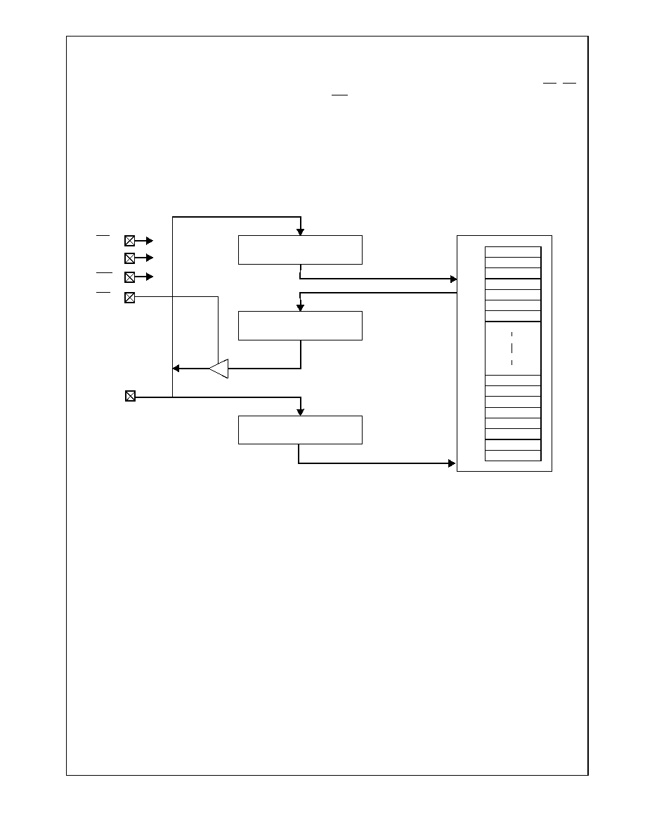
6.0 Parallel Interface
The parallel interface allows the USBN9602 to function as
a CPU or microcontroller peripheral. One of two interface
modes can be selected via the MODE0 pin while the
MODE1 pin is pulled low:
� Non-multiplexed mode
� Multiplexed mode
6.1 Non-Multiplexed Mode
The non-multiplexed mode uses the control pins CS, RD,
WR, the address pin A0, and the bidirectional data bus
D[7:0], as shown in Figure 3. This mode is selected by ty-
ing both the MODE1 and MODE0 pin to GND.
The CPU has direct access to the registers DATA_IN,
DATA_OUT and ADDR. Reading and writing data to the
USBN9602 can be done either in standard or burst mode.
See Figure 4 for timing information on the signal timing in
non-multiplexed mode.
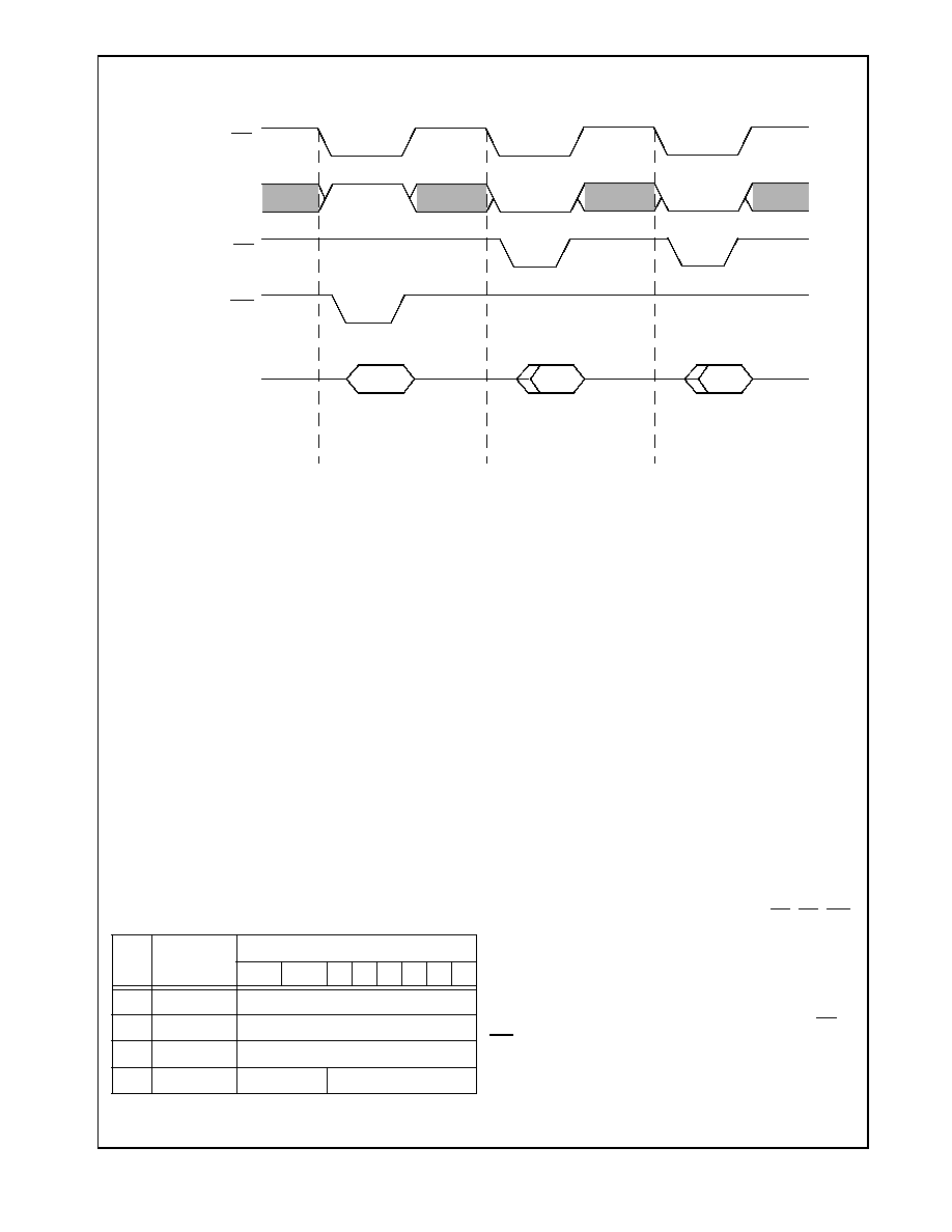
CS
A0
WR
0x00
0x3F
DATA_IN
D[7:0]
RD
DATA OUT
DATA IN
REGISTER FILE
DATA_OUT
ADDR
ADDRESS
Figure 3. Non-Multiplexed Mode Interface Block Diagram
6.0 Parallel Interface
(Continued)
10
www.national.com
6.1.1 Standard Access Mode
The standard USBN9602 access sequence for the non-
multiplexed interface mode is to write the address to the
ADDRESS register and then read or write the data from/to
the DATA_OUT/DATA_IN register. Updating of the
DATA_OUT register occurs following the write of the
ADDR register. Selection between the ADDRESS register
and the DATA_OUT/DATA_IN register is done with the A0
input.
6.1.2 Burst Mode
In burst mode, the ADDR register is written once with the
memory address of the desired on-chip register. Then
consecutive reads/writes are performed to the
DATA_OUT/DATA_IN register without writing a new ad-
dress. The DATA_OUT register contents for read opera-
tions are updated once after every read.
6.1.3 User Registers
The following table gives an overview of the parallel inter-
face registers in non-multiplexed mode. In the table, the
reserved bits return undefined data on read and should be
written with zero.
6.1.4 ADDRESS
The address register (ADDR) acts as a pointer to the in-
ternal memory. This register is write-only and is cleared
upon reset.
6.1.5 DATA_OUT
The Data Output register (DATA_OUT) is updated with the
memory register to which the ADDR register is pointing.
Update occurs under the following conditions:
1. After the ADDR register is written
2. After a read from the DATA_OUT register
3. After a write to the DATA_IN register
This register is read-only and holds undefined data after
reset.
6.1.6 DATA_IN
The Data Input register (DATA_IN) holds the data which is
written to the USBN9602 address ADDR is pointing to.
This register is write-only and is cleared upon reset.
6.2 Multiplexed Mode
The multiplexed mode uses the control pins CS, RD, WR,
the address latch enable signal ALE, and the bidirectional
address data bus AD[7:0], as shown in Figure 6. This
mode is selected by tying MODE1 to GND and MODE0 to
Vcc.
The address is latched into the ADDR register while ALE
is high and data is output/input with the next active RD or
WR signal. All registers are directly accessible in this in-
terface mode. Figure 7 shows the basic timing.
A0
CS
D[7:0]
out
input
RD
WR
out
Write Address
Read Data
Burst Read Data
Figure 4. Non-Multiplexed Mode Basic Timing Diagram
A0
Access
Register Bit Number
7
6
5
4
3
2
1
0
0
read
DATA_OUT
0
write
DATA_IN
1
read
reserved
1
write
reserved
ADDRESS[5:0]

6.0 Parallel Interface
(Continued)
11
www.national.com
CS
WR
0x00
0x3F
AD[7:0]
RD
DATA OUT
DATA IN
REGISTER FILE
ADDR
EN
ADDRESS
Figure 6. Multiplexed Mode Interface Block Diagram
ALE
ALE
CS
AD[7:0]
DATA
RD or WR
ADDR
Figure 7. Multiplexed Mode Basic Read/Write Timing
12
www.national.com
7.0 DMA Support
The USBN9602 supports DMA transfers with an external
DMA controller to and from Endpoints 1 through 6. In this
mode, the device pins DRQ and DACK are used in addi-
tion to the parallel interface pins RD or WR and the data
D[7:0] pins. The DMA mode can only be used with the
parallel interface modes (MODE1 tied to GND). The read
or write address is generated internally and the state of
the A0/ALE pin is ignored during a DMA cycle.
The DMA support logic has a lower priority than the par-
allel interface. CS needs to stay inactive during a DMA cy-
cle. If CS becomes active, DACK is ignored and a regular
read/write operation is performed. Only one Endpoint can
be enabled at a given time to issue a DMA request when
data is received or transmitted.
To enable DMA transfers, the following steps must be per-
formed:
1. The local CPU programs the DMA controller for fly-by
demand mode transfers. In this mode, transfers occur
only when the USBN9602 requests them via the DRQ
pin. The data is read/written from/to the USBN9602 re-
ceive/transmit FIFO and written/read into/from local
memory during the same bus transaction.
2. The DMA address counter is programmed to point to the
destination memory block in the local shared memory,
and the byte count register is programmed with the num-
ber of bytes in the block to be transferred.
3. The DMA request enable bit and DMA source bits are set
in the USBN9602. In addition, the software must set the
respective Endpoint enable bit.
4. The USB host can now perform USB bulk or isochronous
data transfers over the USB bus to the receive FIFO or
from the transmit FIFO in the USBN9602.
5. If the FIFO's warning limit is reached or the transmis-
sion/reception is completed, a DMA request/acknowl-
edge sequence is started for the predetermined number
of bytes. The time at which a DMA request is issued de-
pends on the selected DMA Mode (controlled by the
DMACNTRL.DMOD bit), the current status of the end-
point FIFO, and the FIFO warning enable bits. A DMA re-
quest can be issued immediately.
6. After the DMA controller is granted control of the bus, it
drives a valid memory address and asserts DACK and
RD or WR, thus transferring a byte from the USBN9602
receive FIFO to memory or from memory to the transmit
FIFO. This process continues until the DMA byte count,
within the DMA controller, reaches zero.
7. After the programmed amount of data is transferred, the
firmware needs to do one of the following (depending on
the transfer direction and mode): queue the new data for
transmission by setting the TXCx.TX_EN bit, set the
end-of-packet marker by setting the TXCx.TX_LAST bit,
re-enable reception by setting the RXCx.RX_EN bit, or
check whether the last byte of the packet was received
(RXSx.RX_LAST).
The DMA transfer can be halted at any time by resetting
the USBN9602 DMA request enable bit. If the USBN9602
DMA request enable bit is cleared during the middle of a
DMA cycle, the current cycle is completed before the
DMA request is terminated.
Figure 8 shows the basic DMA read timing and Figure 9
shows the basic DMA write timing.
DACK
DRQ
D[7:0]
WR
input
Figure 8. DMA Write to USBN9602
DACK
DRQ
D[7:0]
RD
output
Figure 9. DMA Read from USBN9602

13
www.national.com
8.0 MICROWIRE/PLUS Interface
The MICROWIRE/PLUS interface allows the USBN9602
to function as a peripheral of a CPU or microcontroller via
a serial interface. This mode is selected by pulling the
MODE1 pin high and the MODE0 pin low. The MICROW-
IRE/PLUS mode uses pins called chip select (CS), serial
clock (SK), serial data in (SI), and serial data out (SO), as
shown in Figure 10.
The MICROWIRE interface is enabled by a falling edge of
CS and reset with a rising edge of CS. Data on SI is shift-
ed in after the rising edge of SK and data is shifted out on
SO after the falling edge of SK. Data transfer from and to
the shift register is done after the falling edge of the eighth
SK clock. Data is transferred with the most significant bit
first. Table 1 summarizes the available commands for the
MICROWIRE interface.
Note: A write operation to any register always reads out the contents of the
register after the write occurs and shifts out that data in the next cycle. This
read does not clear the bit in the respective register, even for a clear-on-read
("Cor") type bit. An exception is writing to the TXDx (transmit data) registers,
which causes undefined data to be read out during the next cycle.
SO
SK
SI
0x00
0x3F
DATA_IN
CS
DATA OUT
DATA IN
REGISTER FILE
DATA_OUT
ADDR
ADDRESS
Figure 10. MICROWIRE Interface Block Diagram
SHIFT REG
CMD[1:0]
SYNC
8.0 MICROWIRE/PLUS Interface
(Continued)
14
www.national.com
Reading the data is done by shifting in the 2-bit command
(CMD) and the 5-bit address (RADDR or WADDR) while
simultaneously shifting out read data from the previous
address.
Writing data can be done in standard mode or burst
mode. The standard mode requires two bytes: the com-
mand and address being shifted in and the data being
shifted in. In burst mode, the command and address are
transferred first, and then consecutive data is written to
that address. The burst mode is terminated by CS going
inactive (high).
For the MICROWIRE interface, Figure 11 shows the basic
read timing, Figure 12 shows the standard write timing,
and Figure 13 shows the write timing in burst mode.
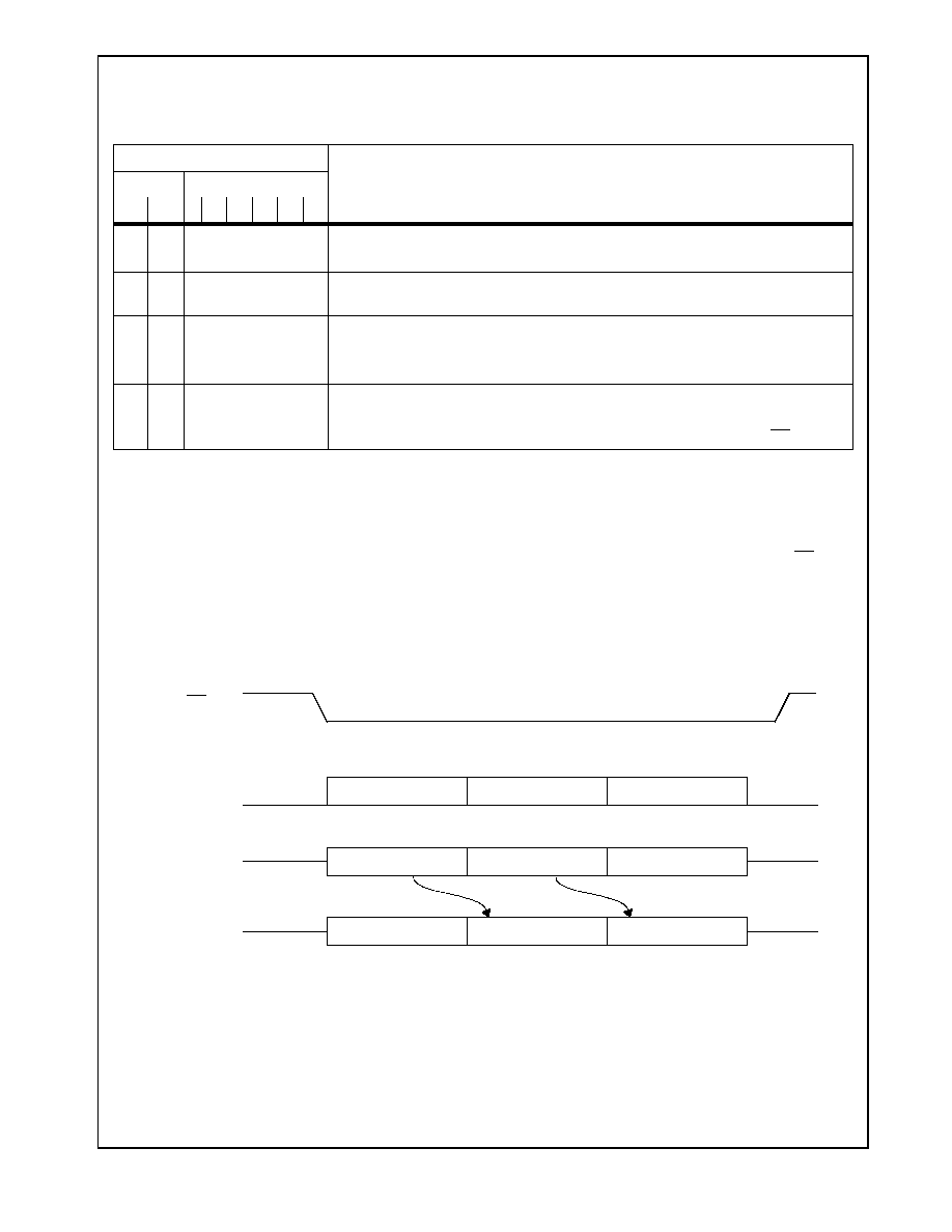
Table 1. MICROWIRE Command/Address Byte Format
Byte Transferred
Sequence initiated. One cycle equals eight SK clocks. Data is transferred after the
eighth SK. clock of one cycle.
CMD
ADDR
1
0
5
4
3
2
1
0
0
0
RADDR
(read)
Cycle 1:
Cycle 2:
Shift in CMD/RADDR; shift out previous read data
Shift in next CMD/ADDR; shift out RADDR data
0
1
x
Cycle 1:
No action; shift out previous read data (does not clear CoR bits)
1
0
WADDR
(normal write)
Cycle 1:
Cycle 2:
Shift in CMD/WADDR; shift out previous read data
Shift in WADDR write data; shift out WADDR read data (does
not clear CoR bits)
1
1
WADDR
(burst write)
Cycle 1:
Cycle 2-n:
Shift in CMD/WADDR; shift out previous read data
Shift in WADDR write data; shift out WADDR read data (does
not clear CoR bits); terminate this mode by pulling CS high
CS
SK
SO
8 Cycles
SI
8 Cycles
8 Cycles
CMD = 0x ADDR CMD = 0x ADDR
new command
undefined data
Read Data
Read Data
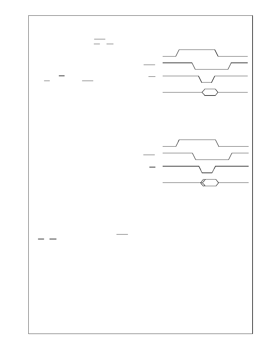
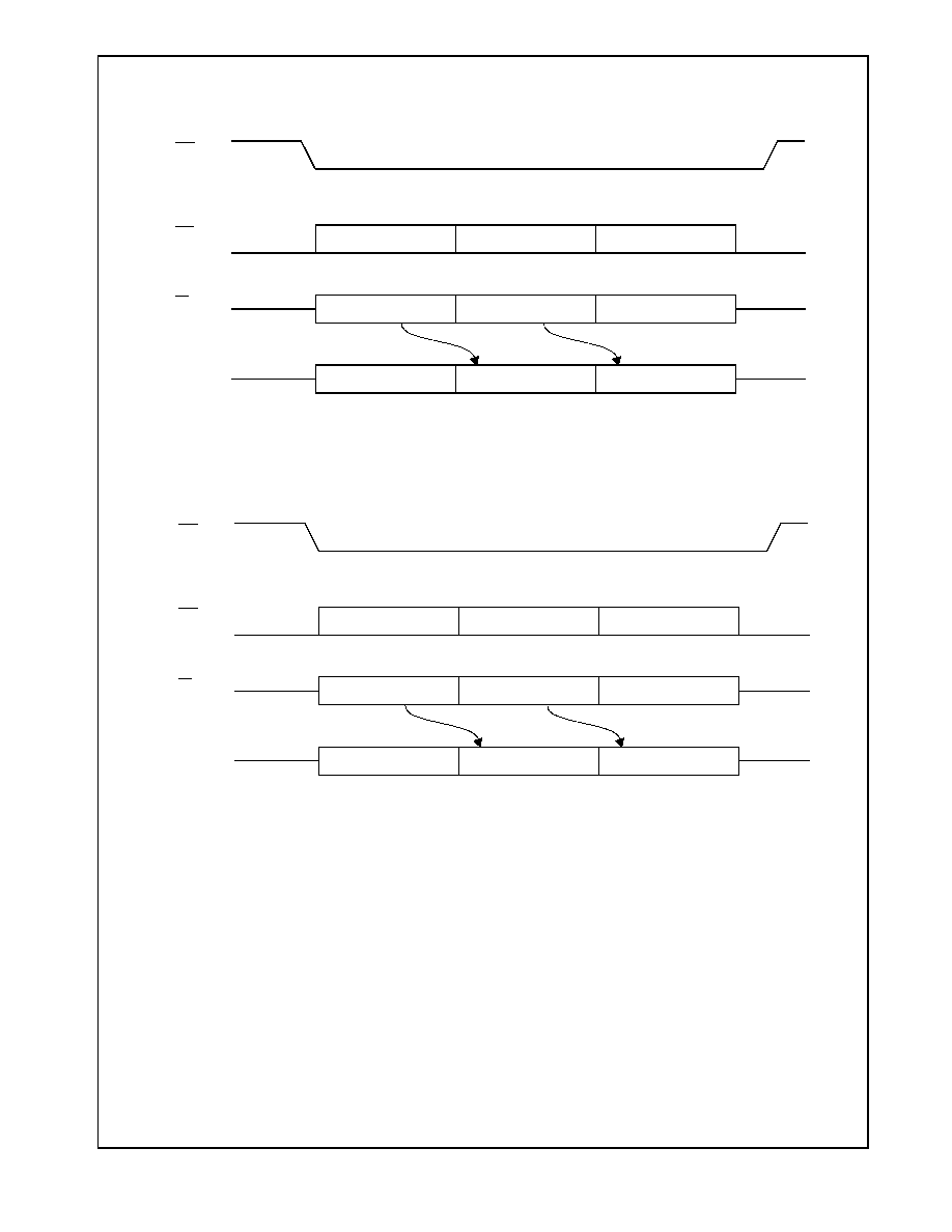
Figure 11. MICROWIRE Interface Basic Read Timing
8.0 MICROWIRE/PLUS Interface
(Continued)
15
www.national.com
CS
SK
SO
8 Cycles
SI
8 Cycles
8 Cycles
CMD = 10 ADDR
Write Data
new command
- undefined data -
Read Data
Read Data
Figure 12. MICROWIRE Interface Standard Write Timing
CS
SK
SO
8 Cycles
SI
8 Cycles
8 Cycles
CMD=11 ADDR
Write Data
Write Data
- undefined data -
Read Data
Read Data
Figure 13. MICROWIRE Interface Burst Write Timing

16
www.national.com
9.0 Device Functional States
At any given time, the USBN9602 operates in one of the
following states:
� "NodeReset" the device is reset
� "NodeOperational" when the device is operating nor-
mally
� "NodeSuspend" when the device is suspended due to
USB inactivity
� "NodeResume" when the device wakes up from the
suspended state
The Suspend, Resume, or Reset line condition causes a
transition from one operating state to another. These con-
ditions are detected by specialized hardware and reported
via the Alternate Event (ALTEV) register. If interrupts are
enabled, an interrupt is generated upon the occurrence
any of the specified condition.
9.1 Suspend Operation
A USB device is expected to enter the Suspend state in
response to the Suspend event, which occurs when 3 ms
has elapsed without any detectable bus activity. The
USBN9602 looks for this event and signals it by setting
the ALTEV.SD3 bit, which causes an interrupt to be gen-
erated. The firmware should respond by putting the
USBN9602 in Suspend state.
In the Suspend state, the transceiver enters a special low-
power mode. All registered states and FIFO Buffers re-
main static so that upon resumption of activity, no addi-
tional operations are necessary.
The USBN9602 can resume operation from the Suspend
state under firmware control as a response to a local
event at the host controller, which can in turn wake up the
USB bus via a remote resume operation, or upon detec-
tion of a resume command on the USB bus that signals
an interrupt to the host controller.
9.2 Remote Resume
If the host has enabled remote wake-ups to occur from
this node, the USBN9602 can initiate a remote wake-up.
Once the firmware detects the event that is supposed to
wake-up the bus, it releases the USBN9602 from the sus-
pend state by initiating a Remote Resume on the USB us-
ing the NFSR register. The node firmware must ensure
that at least 5 ms of Idle has been present on the USB.
While in the Resume state, a constant "K" is signaled on
the USB. This should last for at least 1 ms, after which the
USB host continues sending the resume signal for at least
an additional 20 ms, and then completes the resume op-
eration by issuing the End_Of_Packet (EOP) sequence.
To successfully detect the EOP, the firmware has to enter
the "NodeOperational" state by setting the NFSR register.
Should an End_Of_Packet from the host not be received
within 100 ms, the Remote Resume should be initiated
again by the software.
9.3 USB Resume Operation
Upon detection of resume or reset signal while in the Sus-
pend state, the USBN9602 can signal this to the main
controller by generating an interrupt.
USB specifications requires that a device must be ready
to respond to USB tokens within 10 ms after wake-up or
reset.
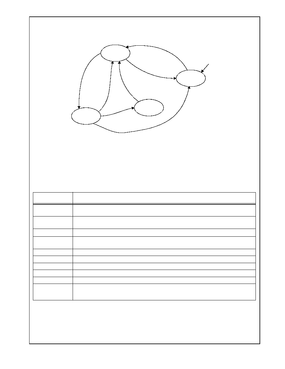
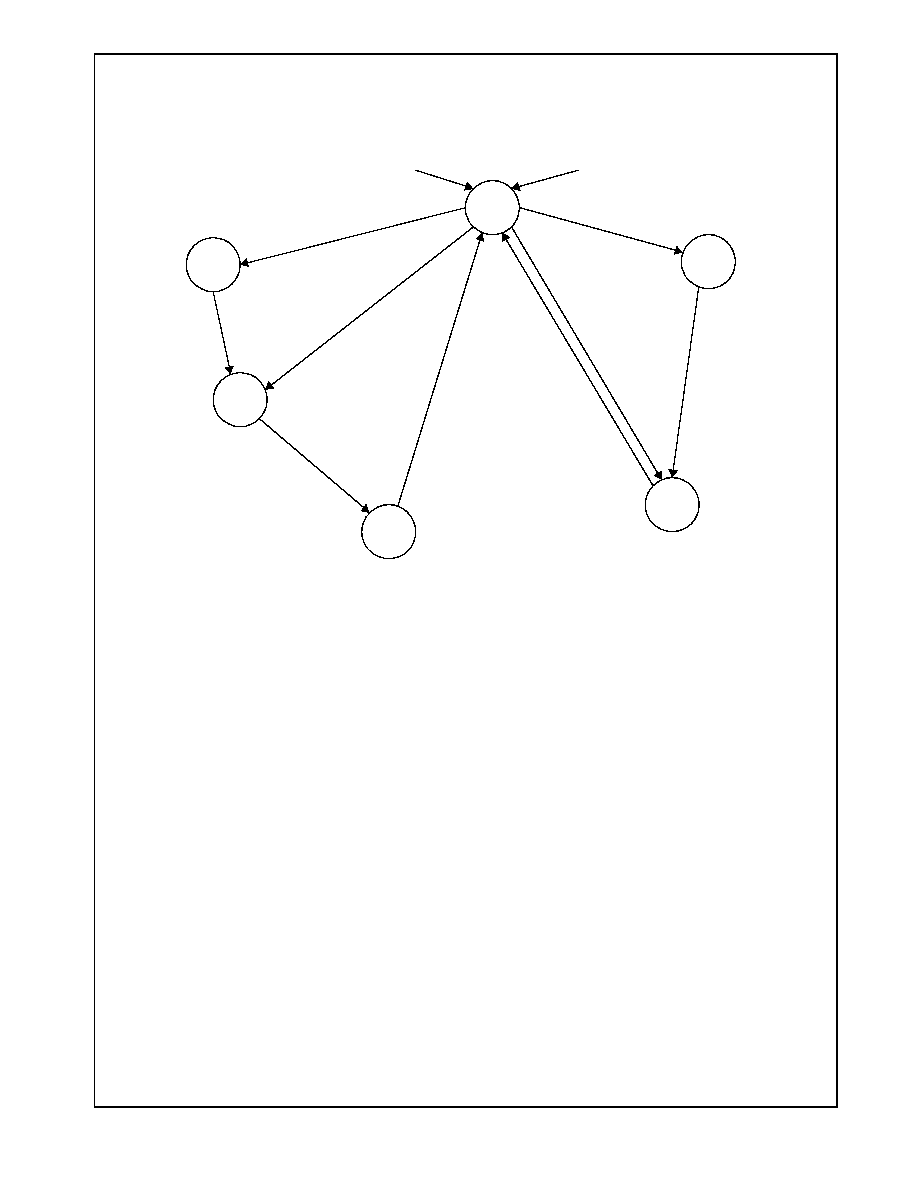
9.4 Functional State Transitions
Figure 14 is a state diagram showing the device states
and transitions. The conditions that trigger each transition
are shown in the figure. Conditions that require firmware
operation are shown in italics. Note that all USBN9602
state transitions are initiated by the firmware.
9.0 Device Functional States
(Continued)
17
www.national.com
The following notes apply to the state diagram:
� When the node is not in the NodeOperational state, all port registers and internal Endpoint states are reset.
� In the NodeResume state, resume signaling is propagated upstream.
� In the NodeSuspend state, the node may enter a low-power state and is able to detect resume signaling.
Table 2 describes the individual conditions that trigger state transitions.
Figure 14. Node Functional State Diagram
Table 2. State Transition Conditions
State
Transition
Condition Asserted
set_reset
Node Functional State register NFS[1:0] bits are written with 00
b
. The firmware should only initiate
set_reset if ALTEV.RESET is set.
set_suspend
Node Functional State register NFS[1:0] bits are written with 11
b
. The firmware should only initiate
set_suspend if ALTEV.SD3 is set.
set_oper
Node Functional State register NFS[1:0] bits are written with 10
b
.
clear_suspend
Node Functional State register NFS[1:0] bits are written with 01
b
.
The firmware should only initiate
clear_suspend if ALTEV.SD5 is set.
reset_det
Alternate Event register RESET bit set (ALTEV.RESET = 1).
local_event
A local event that should wake up the USB.
sd5_det
Alternate Event register SD5 bit set (ALTEV.SD5 = 1).
suspend_det
Alternate Event register SD3 bit set (ALTEV.SD3 = 1).
resume_det
Alternate Event register RESUME bit set (ALTEV.RESUME = 1).
resume_compl
The node should stay in the NodeResume state for at least 10ms and then must enter the Node-
Operational state to detect the EOP from the host, which terminates this remote resume operation.
EOP is indicated by ALTEV.EOP = 1.
10
b
NodeOperational
00
b
NodeReset
01
b
NodeResume
11
b
NodeSuspend
reset_det &
reset_det & set_reset
hw/sw reset
local_event & sd5_detect &
resume_det &
suspend_det &
set_suspend
resume_compl &
set_oper
transition initiated by firmware
set_oper
set_oper
clear_suspend
set_reset
18
www.national.com
10.0 Endpoint Operation
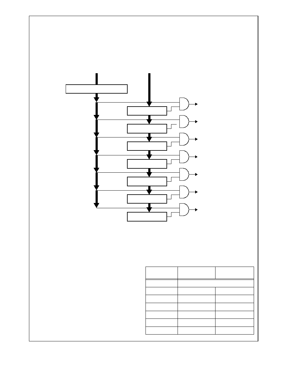
Packets are broadcast from the root hub to all the nodes
on the USB network. Address detection is implemented in
hardware to allow selective reception of packets and to
permit optimal use of microcontroller bandwidth. One
function address with seven different endpoint combina-
tions is decoded in parallel. If a match is found, then that
particular packet is received into the FIFO; otherwise it is
ignored.
The incoming USB Packet Address Field and Endpoint
Field are extracted from the incoming bit stream. Then the
address field is compared to the Function Address Regis-
ter (FADR) and if a match is detected, the Endpoint Field
is compared to all of the Endpoint Control Registers
(EPCx) in parallel. A match will then cause the payload
data to be received or transmitted using the respective
Endpoint FIFO.
10.1 Transmit and Receive Endpoint FIFOs
The USBN9602 uses a total of seven Transmit and Re-
ceive FIFOs. There is one bidirectional Transmit and Re-
ceive FIFO for the mandatory control endpoint zero, plus
an additional three transmit and three receive FIFOs, for
up to six additional endpoints. As shown in Table 3, the
bidirectional FIFO for endpoint zero is 8 bytes deep and
the additional unidirectional FIFOs are 32 or 64 bytes
deep for both transmit and receive. Each FIFO can be
programmed for one exclusive USB endpoint used togeth-
er with one globally decoded USB function address. The
firmware must not have both transmit and receive enabled
for endpoint zero at any given time.
match
EPC0 Reg.
EPC1 Reg.
EPC2 Reg.
EPC3 Reg.
EPC4 Reg.
EPC5 Reg.
EPC6 Reg.
FADR Register
receive/transmit FIFO0
transmit FIFO1
receive FIFO1
transmit FIFO2
receive FIFO2
transmit FIFO3
receive FIFO3
Figure 15. USB Function Address/Endpoint Decoding
match
Table 3. USBN9602 Endpoint FIFO Sizes
Endpoint #
TX FIFO size
(name)
RX FIFO size
(name)
0
8 (FIFO0)
1
32 (TXFIFO1)
-
2
-
32 (RXFIFO1)
3
32 (TXFIFO2)
-
4
-
32 (RXFIFO2)
5
64 (TXFIFO3)
-
6
-
64 (RXFIFO3)
10.0 Endpoint Operation
(Continued)
19
www.national.com
If two endpoints in the same direction are programmed
with the same endpoint number and both are enabled,
then data will be received or transmitted using the end-
point with the lower number until that endpoint gets dis-
abled for BULK or INTERRUPT transfers, or becomes full
or empty for ISO transfers. For example, if receive EP2
and receive EP4 both use the endpoint number five and
are both isochronous, then the first OUT packet is re-
ceived into EP2 and the second OUT packet is received
into EP4, if there is no firmware interaction in between.
For ISO endpoints, this allows implementing a ping-pong
buffer scheme together with the frame number match log-
ic.
Endpoints in different directions programmed with the
same endpoint number still operate independently.
10.2 Bidirectional Control Endpoint FIFO0 Opera-
tion
FIFO0 is intended to be used for the bidirectional control
endpoint zero. It can be configured to receive data sent to
the default address by setting the DEF bit of the EPC0
register. Isochronous transfers are not supported for the
control endpoint.
The Endpoint 0 FIFO can hold a single receive or transmit
packet with up to eight bytes of data. Figure 16 is a state
diagram showing the basic operation of the Endpoint 0
FIFO in both the receive and transmit directions.
Note that the actual current operating state is not directly
visible to the firmware.
A packet written to the FIFO will be transmitted if an IN
token for the respective Endpoint is received. If an error
condition is detected, the packet data remains in the FIFO
and transmission is retried with the next IN token.
The FIFO contents can be flushed to allow response to an
OUT token or to write new data into the FIFO for the next
IN token.
If an OUT token is received for the FIFO, the firmware will
be informed about data being received to the FIFO only if
there was no error condition (CRC or STUFF error). Erro-
neous receptions are automatically discarded.
10.3 Transmit Endpoint FIFO Operation
(TXFIFO1, TXFIFO2, TXFIFO3)
The Transmit FIFOs for Endpoints 1, 3, and 5 support
Bulk, Interrupt, and Isochronous USB transfers of packets
that are greater than the FIFO size. Therefore, the firm-
ware must update the FIFO contents while the USB pack-
et is being transmitted on the bus. Figure 17 illustrates the
operation of the transmit FIFOs.
Figure 16. Endpoint 0 Operation
TxFill
TxWait
Tx
RxWait
Rx
Idle
write to TXD0
TXC0.TX_EN &
RXC0.RX_EN
OUT or
SETUP token
SETUP token
FIFO0 empty
RXC0.FLUSH
TXC0.FLUSH
IN token
transmission
done
(all data read)
TXC0.TX_EN
0-length pkt.
10.0 Endpoint Operation
(Continued)
20
www.national.com
The diagram labels used in Figure 17 are explained be-
low.
10.3.1 TFxS
Transmit FIFO x Size. This is the total number of bytes
available within the FIFO.
10.3.2 TXRP
Transmit Read Pointer. This pointer is incremented every
time the Endpoint controller reads data from the Transmit
FIFO. This pointer wraps around to zero if TFxS is
reached. TXRP is never incremented beyond the value of
the write pointer TXWP.
An underrun condition occurs if TXRP equals TXWP and
an attempt is made to transmit more bytes with the TX-
Cx.LAST bit not set.
10.3.3 TXWP
Transmit Write Pointer. This pointer is incremented every
time the firmware writes to the Transmit FIFO. This pointer
wraps around to zero if TFxS is reached.
If the attempt is made to write more bytes to the FIFO
than actual space is available (FIFO overrun), the write to
the FIFO is ignored. You should therefore check TCOUNT
to obtain an indication of the number of empty bytes re-
maining.
10.3.4 TxFL
Transmit FIFO Level. This value indicates how many bytes
not yet transmitted remain in the FIFO before an underrun
condition occurs on the next read of the FIFO.
A FIFO warning can be issued if TxFL decreases to a
specific value. The respective FWEV.TXWARNx bit is set
if TxFL is equal to or less than the number specified with
TXCx.TFWL.
10.3.5 TCOUNT
Transmit FIFO Count. This value indicates how many
empty bytes are available to be filled within the Transmit
FIFO. This value is accessible by the firmware via the
TXSx Register.
10.4 Receive Endpoint FIFO Operation (RXFIFO1,
RXFIFO2, RXFIFO3)
The Receive FIFOs for Endpoints 2, 4, and 6 support
Bulk, Interrupt, and Isochronous USB transfers of packets
that are greater than the FIFO size. If the packet length
exceeds the FIFO size, the firmware must read the FIFO
contents while the USB packet is being received on the
bus. Figure 18 shows the detailed behavior of the Receive
FIFOs.
The diagram labels used in Figure 18 are explained be-
low.
0x0
+
TXRP
TXWP
TFL = TXWP - TXRP
Tx FIFO X
+
+
TFxS - 1
TCOUNT = TXRP - TXWP (= TFxS - TxFL)
FLUSH (resets TXRP and TXWP)
Figure 17. Tx FIFO Operation
10.0 Endpoint Operation
(Continued)
21
www.national.com
10.4.1 RFxS
Receive FIFO x Size. This is the total number of bytes
available within the FIFO.
10.4.2 RXRP
Receive Read Pointer. This pointer is incremented every
time the firmware reads from the Receive FIFO. This
pointer wraps around to zero if RFxS is reached. RXRP is
never incremented beyond the value of RXWP.
If the attempt is made to read more bytes than are actual-
ly available (FIFO underrun), the last byte is read repeti-
tively. You should therefore check RCOUNT to obtain an
indication of the number of received bytes remaining.
10.4.3 RXWP
Receive Write Pointer. This pointer is incremented every
time the Endpoint controller writes to the Receive FIFO.
This pointer wraps around to zero if RFxS is reached.
A overrun condition occurs if RXRP equals RXWP and an
attempt is made to receive more bytes.
10.4.4 RxFL
Receive FIFO Level. This value indicates how many more
bytes can be received until an overrun condition occurs
with the next write to the FIFO.
A FIFO warning can be issued if RxFL decreases to a
specific value. The respective FWEV.RXWARNx bit is set
if RxFL is equal to or less than the number specified with
RXCx.RFWL.
10.4.5 RCOUNT
Receive FIFO Count. This value indicates how many
bytes are available to be read out of the Receive FIFO.
This value is accessible by the firmware via the RFSx
Register.
10.5 Programming Model
Figure 19 illustrates the register hierarchy. It shows the re-
lationship between the endpoint registers and event regis-
ters.
Figure 18. Rx FIFO Operation
0x0
+
RXRP
RXWP
RFL = RXRP - RXWP (= RFxS - RCOUNT)
Rx FIFO X
+
+
RFxS - 1
FLUSH (resets RXRP and RXWP)
RCOUNT = RXWP - RXRP
10.0 Endpoint Operation
(Continued)
22
www.national.com
EPCy
TXSTA0
MAEV
FIFO0
TXC0
TXFD0
RXSTA0
RXC0
RXFD0
EPC0
8 byte
xxx
Other user-accessible registers
TXSTAx
TXCx
TXFDx
RXCx
RXFDx
RFIFOy
16/32 byte
EPCx
TFIFOx
16/32 byte
TXEV
RXEV
NAK
AEV
Figure 19. Register Hierarchy
FWEV
RXSTAx
23
www.national.com
11.0 Register Set
The USBN9602 has a set of memory-mapped registers
that can be read or written to control the USB interface.
Some register bits are reserved. Reading reserved regis-
ters bits returns undefined data. Reserved register bits
should be always written with zero.
The following conventions are used to describe the regis-
ter format:
11.1 Main Control Register (MCNTRL)
11.1.1 SRST
Software Reset. Setting this bit causes a software reset of
the device. This reset is equivalent to a hardware reset
except that the clock configuration register is unaffected.
Note that the software reset bit clears itself at the end of
the initiated reset operation.
11.1.2 VGE
Voltage Regulator Enable. Setting this bit enables the in-
ternal 3.3V voltage regulator. This bit is hardware reset to
0, disabling the internal 3.3V regulator by default. When
the internal 3.3V regulator is disabled, the device is effec-
tively disconnected from the USB. Upon power-up, the
firmware may perform any needed initialization (such as
power-on self test) and then set the VGE bit. Until the
VGE bit is set, the upstream hub port will not detect the
presence of the device.
If the VGE bit is reset, an external 3.3V power supply may
be used on the V3.3 pin.
11.1.3 NAT
Node Attached. This bit, when set, indicates that this node
is ready to be detected as attached to the USB. When re-
set, the transceiver forces SE0 on the USB port to prevent
the Hub (to which this node is connected) from detecting
an attach event. After reset, this bit is left cleared to allow
the device time before having to respond to commands.
After this bit is set, the device no longer drives the USB
and should be ready to receive Reset signaling form the
hub.
The NAT bit should be set by the firmware only if an ex-
ternal 3.3V supply has been provided to the V3.3 pin, or
at least 1 msec after the VGE bit is set (in the latter case
the delay allows the internal regulator sufficient time to be-
come stable).
11.1.4 INTOC
Interrupt Output Control bits 1 and 0. These bits control
the Interrupt Output pin characteristics according to the
following table.
11.2 Clock Configuration Register (CCONF)
11.2.1 CLKDIV
External clock divisor. The value in this field sets the clock
frequency at the CLKOUT output pin as follows:
frequency = 48 MHz / (CLKDIV+1)
A hardware reset configures the divisor to 11 decimal
which yields a 4 MHz output clock. If the CLKDIV value is
changed by the firmware, the clock output period is ex-
panded or shortened in its current phase for glitch-free
switching.
11.2.2 CODIS
Clock Output Disable. Setting this bit disables the clock
output. When this bit is set, the CLKOUT output pin is fro-
zen in its current state.
bit number
bit or field name (res = reserved)
reset value
read/write characteristics:
r = register bit is read-only
w = register bit is write-only
r/w = register bit is read and written
by firmware
CoR = register bit is cleared if read
HW = register bit can be modified by
device and firmware
bit 7
bit 6
bit 5 bit 4
bit 3
bit 2
bit 1
bit 0
INTOC[1:0]
res
NAT
VGE
res
SRST
0
0
�
0
0
�
0
r/w
�
r/w
r/w
�
r/w
Table 4. INTOC Bit Definition
INTOC
Interrupt Output
1
0
0
0
Disabled (active-high, open drain)
0
1
active-low open drain
1
0
active-high push-pull
1
1
active-low push-pull
bit 7
bit 6
bit 5
bit 4
bit 3
bit 2
bit 1
bit 0
CODIS
res
CLKDIV[3:0]
0
�
1
0
1
1
r/w
�
r/w
11.0 Register Set
(Continued)
24
www.national.com
11.3 DMA Control Register (DMACNTRL)
11.3.1 DSRC
DMA Source. The DMA source bit field holds the binary
encoded value that specifies which one of Endpoints 1 to
6 is enabled for DMA support. The DSRC bits are cleared
upon reset. Table 5 summarizes the DSRC bit settings.
11.3.2 DMOD
DMA Mode. This bit specifies the time at which a DMA re-
quest is issued.
If the DMOD bit is 0, a DMA request is issued upon trans-
fer completion. For transmit endpoints EP1, EP3, and
EP5, this is the time at which the data is completely trans-
ferred as indicated by the TX_DONE bit. For receive End-
points EP2, EP4, and EP6, this is the time at which the
data is completely transferred as indicated by the
RX_LAST bit. If the DMOD bit is 1, a DMA request is is-
sued when the respective FIFO warning bit is set.
A DMA request from a transmit endpoint remains activat-
ed until the request condition goes away. If DMOD is
cleared to 0, DMA requests will be issued until the firm-
ware reads the respective transmit status register (TXSx)
and thus resets the TX_DONE bit, or if the TX-
Cx.TX_LAST bit in the transmit command register gets set
by the firmware. If DMOD is set to 1, DMA requests will
be issued until the FIFO warning condition goes away as
a result of sufficient bytes being transferred to the end-
point, or if the TX_DONE bit get set as a result of a trans-
mission.
DMA requests from a receive endpoint remains activated
until the request condition goes away. If DMOD is cleared
to 0, DMA requests will be issued until the firmware reads
the respective receive status register (RXSx) and thus re-
sets the RX_LAST bit, or if the endpoint FIFO becomes
empty due to sufficient reads. If DMOD is set to 1, DMA
requests will be issued until the FIFO warning condition
goes away, or the FIFO is flushed.
If DMOD is cleared to 0 (and the endpoint and DMA are
enabled), DMA requests will be issued until the firmware
reads the respective transmit/receive status register (TX-
Cx or RXCx) and thus resets the TX_DONE/RX_LAST bit.
If DMOD is set to 1 (and the endpoint and DMA are en-
abled), DMA requests will be issued until the FIFO warn-
ing condition goes away.
11.3.3 DEN
DMA Enable. This bit enables the DMA support mode
when set. If this bit is reset and the current DMA cycle is
completed or not yet issued, the DMA transfer is terminat-
ed. When the USBN9602 operates is in the MICROWIRE
interface mode, DMA operation cannot be enabled and
setting this bit does not have any effect.
11.4 Revision Identifier Register (RID)
11.4.1 REVID
This register holds the binary encoded chip revision. For
this revision it holds 0001
b
.
11.5 Node Functional State Register (NFSR)
11.5.1 NFS
Node Functional State bits. The firmware should initiate all
required state transitions according to the respective sta-
tus bits in the Alternate Event register. The valid transi-
tions are shown in the "Node Functional State Diagram"
on page 17. The NFS bits set the node state as follows:
NFS[1:0] = 00 : NodeReset
NFS[1:0] = 01 : NodeResume
NFS[1:0] = 10 : NodeOperational
NFS[1:0] = 11 : NodeSuspend
bit 7
bit 6
bit 5
bit 4
bit 3
bit 2
bit 1
bit 0
DEN
res
DMOD
DSRC[2:0]
0
�
0
0
0
0
r/w
�
r/w
r/w
Table 5. DSRC Bit Description
DSRC
Endpoint #
2
1
0
0
0
0
1
0
0
1
2
0
1
0
3
0
1
1
4
1
0
0
5
1
0
1
6
1
1
x
reserved
bit 7
bit 6
bit 5
bit 4
bit 3
bit 2
bit 1
bit 0
reserved
REVID[3:0]
�
0
0
0
0
�
r
bit 7
bit 6
bit 5
bit 4
bit 3
bit 2
bit 1
bit 0
res
NFS[1:0]
�
0
0
�
r/w

11.0 Register Set
(Continued)
25
www.national.com
"NodeReset" is the USB Reset state. This is entered upon
a module reset or by software upon detection of a USB
Reset. Upon entry, all Endpoint Pipes are disabled.
EPC0.DEF and FAR.AD_EN should be cleared by the
software upon entry into this state. Upon exit from this
state, EPC0.DEF should be set so that the device re-
sponds to the default address.
"NodeResume" is the state in which Resume "K" signal-
ling is generated. The firmware should cause a transition
to this state to initiate a remote wake-up sequence by the
device. The node must remain in this state for at least 1
ms and no more than 15 ms.
"NodeOperational" is the normal operational state. In this
state the node is configured for operation on the USB.
"NodeSuspend" is the device inactive state. The firmware
should cause a transition to this state upon detection of a
Suspend event while in the NodeOperational state. While
in the NodeSuspend state, the transceivers operate in
their low-power suspend mode. All Endpoint Controllers
and internal states remain frozen. Upon detection of bus
activity, the ALTEV.RESUME bit is set. In response, soft-
ware can cause an entry to the NodeOperational state.
11.6 Main Event Register (MAEV)
11.6.1 WARN
FIFO Warning. One of the unmasked bits in the FIFO
Warning Event register has been set. The WARN bit is
cleared by reading the FIFO Warning Event Register.
11.6.2 ALT
Alternate Event. One of the unmasked bits in the Alter-
nate Event register has been set. The ALT bit is cleared
when the Alternate Event register is read.
11.6.3 TX_EV
Transmit Event. This bit is set if any of the unmasked bits
in the Transmit Event register (TXFIFOx or TXUNDRNx)
are set. Therefore, it indicates that an IN transaction has
been completed. This bit is cleared when all the
TX_DONE bits and the TXUNDRN bits in each Transmit
Status register are cleared.
11.6.4 FRAME
Frame event. This bit is set if the frame counter is updated
with a new value. This can be due to a valid SOF packet
being received on the USB or due to an artificial update if
the frame counter was unlocked or a frame was missed.
This bit is cleared when the register is read.
11.6.5 NAK
NAK Handshake. This bit is set if one of the unmasked
NAK Event register bits has been set. This bit is cleared
when the NAK Event register is read.
11.6.6 ULD
Unlock Locked Detected. If set, this bit indicates that the
Frame Timer has entered the unlocked state from a
locked condition, or has re-entered the locked condition
from an unlocked condition, as determined by the Un-
locked Status bit (FN.UL) being currently set. This bit is
cleared when the register is read.
11.6.7 RX_EV
Receive Event. This bit is set if any of the unmasked bits
in the Receive Event register are set. It indicates that a
SETUP or OUT transaction has been completed. This bit
is cleared when all of the RX_LAST bits in each of the re-
ceive status registers and all of the RXOVRRN bits in the
receive event register are cleared.
11.6.8 INTR
Master Interrupt Enable. This bit is hard-wired to zero in
the Main Event register. However, the corresponding bit in
the Main Mask register is the master interrupt enable.
11.7 Main Mask Register (MAMSK)
A bit is set to 1 in the Main Mask register enables gener-
ation of an interrupt on the occurrence of the respective
event in the Main Event register. Interrupt generation is
disabled otherwise. For information on the individual inter-
rupt events, see the description of the Main Event register.
11.8 Alternate Event Register (ALTEV)
11.8.1 SD3
Suspend Detect 3 ms. This bit is set after 3 milliseconds
of idle time is detected on the upstream port, indicating
that the device should be suspended. The suspend oc-
curs under firmware control by writing the SUSPEND val-
ue to the NFS register. The SD3 bit is cleared when the
register is read.
bit 7
bit 6
bit 5 bit 4
bit 3
bit 2
bit 1
bit 0
INTR RX_EV ULD NAK FRAME TX_EV ALT WARN
0
0
0
0
0
0
0
0
see
text
r
CoR
r
CoR
r
r
r
bit 7
bit 6
bit 5 bit 4
bit 3
bit 2
bit 1
bit 0
INTR RX_EV ULD NAK FRAME TX_EV ALT WARN
0
0
0
0
0
0
0
0
r/w
bit 7
bit 6
bit 5
bit 4
bit 3 bit 2 bit 1 bit 0
RESUME
RESET SD5 SD3 EOP
res
0
0
0
0
0
�
CoR
CoR
CoR CoR CoR
�
11.0 Register Set
(Continued)
26
www.national.com
11.8.2 SD5
Suspend Detect 5 ms. This bit is set after 5 milliseconds
of idle time is detected on the upstream port, indicating
that this device is now permitted to perform a remote
wake-up operation. The resume operation may be initiated
under firmware control by writing the RESUME value to
the NFS register. The SD5 bit is cleared when the register
is read.
11.8.3 RESET
Reset. This bit is set when 2.5
�
sec of SEO is detected
on the upstream port. In response, the functional state
bits (NFSR.NFS) should be written with 00 to reset the
device, and the device should remain in the reset state for
at least 100
�
sec. After being reset, the functional state
may be returned to the operational state. The RESET bit
is cleared when the register is read.
11.8.4 RESUME
Resume. This bit is set when resume signaling is detected
on the USB while this device is in the Suspend state (NF-
SR.NFS = 11), indicating that this device should begin its
wake-up sequence and enter the operational state. The
RESUME bit is cleared when the register is read.
11.8.5 EOP
End of Packet. This bit is set when a valid End of Packet
sequence is detected on the USB. This bit is used when
this device has initiated a Remote wake-up sequence to
indicate that the resume sequence has been acknowl-
edged and completed by the host. The EOP bit is cleared
when the register is read.
11.9 Alternate Mask Register (ALTMSK)
A bit is set to 1 in the Alternate Mask register enables au-
tomatic setting of the MAEV.ALT bit in the Main Event reg-
ister on the occurrence of the respective event in the
Alternate Event register. Setting of the MAVE.ALT bit is
disabled otherwise. For information on the individual alter-
nate events, see the description of the Alternate Event
register.
11.10 Transmit Event Register (TXEV)
11.10.1 TXFIFO
Transmit FIFO. These bits are copies of the TX_DONE
bits from the corresponding Transmit Status registers. The
bits are set when the IN transaction for the corresponding
transmit endpoint is completed. The bits are cleared when
the corresponding Transmit Status register is read.
11.10.2 TXUDRRN
Transmit Underrun. These bits are copies of the respec-
tive TX_URUN bits from the corresponding Transmit Sta-
tus registers. Whenever any of the Transmit FIFOs
underflow, the respective TXUDRRN bit is set. These bits
are cleared when the corresponding FIFOx Transmit Sta-
tus register is read.
As Endpoint 0 implements a store and forward principle,
an underrun condition for FIFO0 cannot occur. Thus, the
TXUDRRN0 bit is always zero.
11.11 Transmit Mask Register (TXMSK)
A bit is set to 1 in the Transmit Mask register enables au-
tomatic setting of the MAEV.TX_EV bit in the Main Event
register on the occurrence of the respective event in the
Transmit Event register. Setting of the MAVE.TX_EV bit is
disabled otherwise. For information on the individual trans-
mit events, see the description of the Transmit Event reg-
ister.
bit 7
bit 6
bit 5
bit 4
bit 3
bit 2 bit 1 bit 0
RESUME
RESET SD5 SD3 EOP
res
0
0
0
0
0
res
r/w
bit 7
bit 6
bit 5
bit 4
bit 3
bit 2
bit 1
bit 0
TXFI
FO3
TXFI
FO2
TXFI
FO1
FIFO
0
TXFIF
O3
TXFIF
O2
TXFIF
O1
FIF
O0
TXUDRRN[3:0]
TXFIFO[3:0]
0
0
0
0
0
0
0
0
r
see
text
r
bit 7
bit 6
bit 5
bit 4
bit 3
bit 2
bit 1
bit 0
TXUDRRN[3:0]
TXFIFO[3:0]
0
0
0
0
0
0
0
0
r/w
11.0 Register Set
(Continued)
27
www.national.com
11.12 Receive Event Register (RXEV)
11.12.1 RXFIFO
Receive FIFO. This bit is set whenever either RX_ERR or
RX_LAST in the respective Receive Status register is set.
Reading the corresponding Receive Status register auto-
matically clears this bit.
The USBN9602 implementation discards all packets for
Endpoint 0 received with errors. This is necessary, in the
case of retransmission due to media errors, to ensure that
a good copy of a SETUP packet is captured. Otherwise,
the FIFO could be tied up holding corrupted data and un-
able to receive a retransmission of the same packet.
Therefore, the RXFIFO0 bit only reflects the value of
RX_LAST (and not RX_ERR) for endpoint 0.
If data streaming is used for the receive endpoints (EP2,
EP4, and EP6), the firmware needs to check with the re-
spective RX_ERR bits to ensure that the packets received
are not corrupted by errors.
11.12.2 RXOVRRN
Receive Overrun. This bit is set in the event of a FIFO
overrun condition. This bit is cleared when the register is
read.
11.13 Receive Mask Register (RXMSK)
A bit is set to 1 in the Receive Mask register enables au-
tomatic setting of the MAEV.RX_EV bit in the Main Event
register on the occurrence of the respective event in the
Receive Event register. Setting of the MAVE.RX_EV bit is
disabled otherwise. For information on the individual re-
ceive events, see the description of the Receive Event
register.
11.14 NAK Event Register (NAKEV)
11.14.1 IN
In Token NAK. This bit is set to 1 when a NAK handshake
is generated for an enabled address/endpoint combination
(FAR.AD_EN = 1 and EPCx.EP_EN = 1) in response to
an IN token. This bit is cleared when the register is read.
11.14.2 OUT
Out Token NAK. This bit is set to 1 when a NAK hand-
shake is generated for an enabled address/endpoint com-
bination (FAR.AD_EN = 1 and EPCx.EP_EN = 1) in
response to an OUT token. This bit is not set if NAK is
generated as result of an overrun condition. This bit is
cleared when the register is read.
11.15 NAK Mask Register (NAKMSK)
A bit is set to 1 in the NAK Mask register enables auto-
matic setting of the MAEV.NAK bit in the Main Event reg-
ister on the occurrence of the respective event in the NAK
Event register. Setting of the MAEV.NAK bit is disabled
otherwise. For information on the individual NAK events,
see the description of the NAK Event register.
11.16 FIFO Warning Event Register (FWEV)
11.16.1 TXWARN
Transmit FIFO Warning. This bit is set to 1 when the re-
spective Transmit Endpoint FIFO reaches the warning limit
as specified by the TFWL bits of the respective Transmit
Command register and transmission from the respective
endpoint is enabled. This bit is cleared when the warning
condition is cleared by writing new data to the FIFO, by
flushing the FIFO, or when the transmission is done as in-
dicated by the TX_DONE bit within the Transmit Status
register.
bit 7
bit 6
bit 5
bit 4
bit 3
bit 2
bit 1
bit 0
RXFIFO3 RXFIFO2 RXFIFO1 FIFO0 RXFIFO3 RXFIFO2 RXFIFO1 FIFO0
RXOVRRN[3:0]
RXFIFO[3:0]
0
0
0
0
0
0
0
0
CoR
r
bit 7
bit 6
bit 5
bit 4
bit 3
bit 2
bit 1
bit 0
RXOVRRN[3:0]
RXFIFO[3:0]
0
0
0
0
0
0
0
0
r/w
bit 7
bit 6
bit 5
bit 4
bit 3
bit 2
bit 1
bit 0
OUT[3:0]
IN[3:0]
0
0
0
0
0
0
0
0
CoR
CoR
bit 7
bit 6
bit 5
bit 4
bit 3
bit 2
bit 1
bit 0
OUT[3:0]
IN[3:0]
0
0
0
0
0
0
0
0
r/w
bit 7
bit 6
bit 5
bit 4
bit 3
bit 2
bit 1
bit 0
RXFIFO3 RXFIFO2 RXFIFO1
res
TXFIFO3 TXFIFO2 TXFIFO1
res
RXWARN[3:1]
res
TXWARN[3:1]
res
0
0
0
�
0
0
0
�
r
�
r
�

11.0 Register Set
(Continued)
28
www.national.com
11.16.2 RXWARN
Receive FIFO Warning. This bit is set to 1 when the re-
spective Receive Endpoint FIFO reaches the warning limit
as specified by the RFWL bits of the respective Receive
Command register. This bit is cleared when the warning
condition is cleared by reading data from the FIFO or by
flushing the FIFO.
11.17 FIFO Warning Mask Register (FWMSK)
A bit is set to 1 in the FIFO Warning Mask register en-
ables automatic setting of the MAEV.WARN bit in the Main
Event register on the occurrence of the respective event in
the FIFO Warning Event register. Setting of the
MAVE.WARN bit is disabled otherwise. For information on
the individual FIFO warning events, see the description of
the FIFO Warning Event register.
11.18 Frame Number High Byte Register (FNH)
11.18.1 FN
Frame Number. This field contains the highest-order bits
of the current frame number, as received in the last SOF
packet. If a valid frame number is not received within
12060 bit times (FLMAX with tolerance) of the previous
change, the frame number is incremented artificially. If two
successive frames are missed or are incorrect, the current
FN is frozen and loaded with the next frame number from
a valid SOF packet.
The low-order byte of the frame number is contained in
the Frame Number Low Byte register (FNL). The correct
sequence to read the frame number is FNL first, then
FNH. Reading from the FNL register locks the three high-
order bits in the FNH register, ensuring a match between
the low-order and high-order bits.
11.18.2 UL
Unlocked Flag. This bit is set to indicate that at least two
frames were received without an expected frame number
or that no valid SOF was received within 12060 bit times.
If this bit is set, the frame number from the next valid SOF
packet is loaded in FN. Upon reset, this flag is set to 1.
11.18.3 MF
Missed SOF Flag. This bit is set to indicate a discontinuity
in the Frame Number. It is set when the frame number in
a valid received SOF does not match the expected next
value. The flag is also set when an SOF is not received
within 12060 bit times. Upon reset, this flag is set to 1.
11.18.4 RFC
Reset Frame Count. Setting this bit resets the Frame
Number to 0x000 and then clears itself (the RFC bit) to
zero. This bit always reads back as zero.
11.19 Frame Number Low Byte Register (FNL)
The Frame Number Low Byte register (FNL) holds the
low-order byte of the Frame Number (see the description
of the Frame Number High Byte register (FNH). The cor-
rect sequence to read the frame number is FNL first, then
FNH. Reading from the FNL register locks the three high-
order bits in the FNH register, ensuring a match between
the low-order and high-order bits.
11.20 Function Address Register (FAR)
The Function Address register (FAR) sets the function ad-
dress for the device. The different Endpoint numbers are
set for each endpoint individually via the Endpoint Control
registers.
11.20.1 AD
Address. This field holds the 7-bit function address. The
function address is used for transmission and reception of
all tokens addressed to the device.
11.20.2 AD_EN
Address Enable. When set to 1, the bits AD[6:0] are used
in address comparison. See "Endpoint Operation" on
page 18 for details. When cleared, the device does not re-
spond to any token on the USB bus.
Note: If the DEF bit in the Endpoint Control Register 0 is set, Endpoint zero
responds to the default address.
bit 7
bit 6
bit 5
bit 4
bit 3
bit 2
bit 1
bit 0
RXFIFO3 RXFIFO2 RXFIFO1
res
TXFIFO3 TXFIFO2 TXFIFO1
res
RXWARN[3:1]
res
TXWARN[3:1]
res
0
0
0
0
0
0
0
0
r/w
bit 7
bit 6
bit 5
bit 4
bit 3
bit 2
bit 1
bit 0
MF
UL
RFC
reserved
FN[10:8]
1
1
0
�
0
0
0
r
r
w/r0
�
r
bit 7
bit 6
bit 5
bit 4
bit 3
bit 2
bit 1
bit 0
FN[7:0]
0
0
0
0
0
0
0
0
r
bit 7
bit 6
bit 5
bit 4
bit 3
bit 2
bit 1
bit 0
AD_EN
AD[6:0]
0
0
0
0
0
0
0
0
r/w
r/w

11.0 Register Set
(Continued)
29
www.national.com
11.21 Endpoint Control Register 0 (EPC0)
This register controls the mandatory control endpoint zero.
11.21.1 EP
Endpoint Address. This field holds the 4-bit endpoint ad-
dress. For Endpoint 0, these bits are hard-wired to 0000
b
.
11.21.2 DEF
Default Address. When this bit is set, the device responds
to the default address, regardless of the contents of the
FAR[6:0] and EP0[3:0] fields. When an IN packet is trans-
mitted for the endpoint, the DEF bit is automatically
cleared.
This bit is used in the transition from the default address
to an assigned address. The transition from the default
address 00000000000
b
to an address assigned during
bus enumeration cannot occur in the middle of the
SET_ADDRESS control sequence, in order to allow com-
pletion of the control sequence. However, the address
needs to be changed immediately upon completion of the
SET_ADDRESS control sequence to avoid errors in the
case that another control sequence immediately follows
the SET_ADDRESS command.
Upon USB-Reset, the firmware has 10 mS to set things
up and should write 0x80 to the Function Address Regis-
ter (FAR) and 0x00 to Endpoint Control Register 0
(EPC0). At SET_ADDRESS, the firmware must write 0x40
to EPC0. Then write the assigned function address, logi-
cally ORed with 0x80, to FAR. Then queue a zero-length
IN packet to complete the status phase of the
SET_ADDRESS control sequence.
Note that if a SET_ADDRESS control sequence occurs
when the current function address is not the default, then
the mechanism described above does not work. The firm-
ware must not set the DEF bit in this case, and must not
update the FAR register until the SET_ADDRESS control
sequence completes (including all handshakes).
11.21.3 STALL
Stall Handshake. Setting this bit causes the chip to gener-
ate a STALL handshake under either of the following con-
ditions:
� The transmit FIFO is enabled and an IN token is re-
ceived.
� The receive FIFO is enabled and an OUT token is re-
ceived.
Note that setting this bit does not cause a STALL hand-
shake to be generated in response to a SETUP token.
Upon transmitting the STALL handshake, the RX_LAST or
TX_DONE bit is set in the respective Receive Status or
Transmit Status register.
11.22 Transmit Status Register 0 (TXS0)
11.22.1 TCOUNT
Transmit FIFO Count. This field indicates the count of
empty bytes available in the FIFO. The value in this field
is never larger than eight for Endpoint zero.
11.22.2 TX_DONE
Transmit Done. This bit, when set, indicates that a trans-
mission of a packet has been completed. This bit is
cleared when the register is read.
11.22.3 ACK_STAT
Acknowledge Status. This bit indicates the acknowledge
status (from the host) regarding the ACK for the previously
sent packet. This bit is to be interpreted when TX_DONE
is set to 1. This bit itself is set when an ACK is received;
otherwise it remains cleared. This bit is also cleared when
the register is read.
11.23 Transmit Command Register 0 (TXC0)
11.23.1 TX_EN
Transmit Enable. This bit must be set by the firmware to
start a packet transmission. It is cleared by the chip after
transmitting a single packet or a STALL handshake in re-
sponse to an IN token. Note that the RX_EN bit in the Re-
ceive Command Register 0 takes precedence over this bit.
In other words, as long as the RX_EN bit is set, the
TX_EN bit is ignored.
A zero-length packet is indicated by setting this bit without
writing any data into the FIFO.
11.23.2 TOGGLE
Data Toggle. This bit specifies the type of PID used for
transmitting the packet. A value of 0 causes a DATA0 PID
to be generated, while a value of 1 causes a DATA1 PID
to be generated. This bit is not altered by the hardware.
11.23.3 FLUSH
Flush FIFO. Writing a 1 to this bit flushes all data from the
control endpoint FIFO, resets the Endpoint to IDLE, clears
the FIFO read and write pointer, and then clears itself. If
the endpoint is currently using FIFO0 to transfer data on
the USB, flushing is delayed until after the transfer is
done. This bit is cleared on reset. This bit and the
RXC0.FLUSH bit are equivalent.
bit 7
bit 6
bit 5
bit 4
bit 3
bit 2
bit 1
bit 0
STALL
DEF
res
EP[3:0]
0
0
�
0
0
0
0
r/w
r/w
�
r; hardwired to 0
bit 7
bit 6
bit 5
bit 4 bit 3 bit 2 bit 1 bit 0
res ACK_STAT TX_DONE
TCOUNT[4:0]
�
0
0
0
0
0
0
0
�
CoR
CoR
r
bit 7 bit 6 bit 5
bit 4
bit 3
bit 2
bit 1
bit 0
res
IGN_IN FLUSH TOGGLE
res
TX_EN
�
0
0
0
�
0
�
r/w
r/w HW
r/w
�
r/w HW

11.0 Register Set
(Continued)
30
www.national.com
11.23.4 IGN_IN
Ignore IN Tokens. When this bit is set, the endpoint ig-
nores any IN tokens directed to its configured address.
11.24 Transmit Data Register 0 (TXD0)
11.24.1 TXFD
Transmit FIFO Data Byte. See "Bidirectional Control End-
point FIFO0 Operation" on page 19 for a description of
this type of data handling.
The firmware is expected to write only the packet payload
data. The PID and CRC16 are created automatically.
11.25 Receive Status Register 0 (RXS0)
This is the receive status register for the bidirectional con-
trol endpoint zero. To allow the reception of a SETUP
packet after the reception of a zero-length OUT/SETUP
packet, two copies of this register exist in hardware: one
to hold the receive status of a zero-length packet and an-
other to hold the status of the following SETUP packet
with data. If a zero-length packet is followed by a SETUP
packet, the first read of this register indicates the status of
the zero-length packet (with RX_LAST set and RCOUNT
cleared to zero) and the second read indicates the status
of the SETUP packet.
11.25.1 RCOUNT
Receive FIFO Count. This field indicates the count of
bytes presently in the RX FIFO. The value in this field is
never larger than eight for endpoint zero.
11.25.2 RX_LAST
Receive Last. This bit, when set, indicates that the
RCOUNT field reflects the number of bytes remaining of
the packet. This bit is left unchanged on zero-length pack-
ets. This bit is cleared when the register is read.
11.25.3 TOGGLE
Data Toggle. When set, this bit indicates that the last suc-
cessfully received packet was received with a DATA1 PID.
This bit is cleared if the last successfully received packet
had a DATA0 PID. This bit is left unchanged on zero-
length packets. This bit is also cleared by reading the Re-
ceive Status Register 0.
11.25.4 SETUP
Setup Packet. When set, this bit indicates that a setup
packet has been received. This bit is left unchanged on
zero-length packets. It is cleared when the register is
read.
11.26 Receive Command Register 0 (RXC0)
11.26.1 RX_EN
Receive Enable. Out packet reception is disabled after the
reception of every data packet or when a STALL hand-
shake is returned in response to an OUT token. A 1 must
be written to this bit to re-enable data reception. Recep-
tion of SETUP packets is always enabled. In the case of
back-to-back SETUP packets (for a given endpoint) where
a valid SETUP packet has been received with no other in-
tervening non-SETUP tokens, the Endpoint Controller dis-
cards the new SETUP packet and return an ACK
handshake. If any other reasons prevent the Endpoint
Controller from accepting the SETUP packet, it must not
generate a handshake. This allows recovery from a condi-
tion where the ACK of the first SETUP token is lost by the
host.
11.26.2 IGN_OUT
Ignore OUT Tokens. When this bit is set, the endpoint ig-
nores any OUT tokens directed to its configured address.
11.26.3 IGN_SETUP
Ignore SETUP Tokens. When this bit is se.t the endpoint
ignores any SETUP tokens directed to its configured ad-
dress.
11.26.4 FLUSH
Flush FIFO. Writing a 1 to this bit flushes all data from the
control endpoint FIFO, resets the Endpoint to IDLE, clears
the FIFO read and write pointers, and then clears itself. If
the endpoint is currently using the FIFO0 to transfer data
on the USB, flushing is delayed until after the transfer is
done. This bit is cleared on reset. This bit and the
TXC0.FLUSH bit are equivalent.
bit 7
bit 6
bit 5
bit 4
bit 3
bit 2
bit 1
bit 0
TXFD
don't care
w
bit 7
bit 6
bit 5
bit 4
bit 3 bit 2 bit 1 bit 0
res SETUP TOGGLE RX_LAST
RCOUNT[3:0]
�
0
0
0
0
0
0
0
�
CoR
CoR
CoR
r
bit 7 bit 6 bit 5 bit 4
bit 3
bit 2
bit 1
bit 0
res
FLUSH
IGN_SETUP
IGN_OUT
RX_EN
�
0
0
0
0
�
r/w
HW
r/w
r/w
r/w

11.0 Register Set
(Continued)
31
www.national.com
11.27 Receive Data Register 0 (RXD0)
11.27.1 RXFD
Receive FIFO Data Byte. See "Bidirectional Control End-
point FIFO0 Operation" on page 19 for a description of
this type of data handling.
The firmware should expect to read only the packet pay-
load data. The PID and CRC16 are removed from the in-
coming data stream automatically.
11.28 Endpoint Control Register x (EPC1 through
EPC6)
The six Endpoint Control Registers EPC1 through EPC6
control the configuration of unidirectional endpoints 1
through 6, respectively. Each register follows the format
shown above.
11.28.1 EP
Endpoint Address. This field holds the 4-bit endpoint ad-
dress.
11.28.2 EP_EN
Endpoint Enable. When this bit is set, the bits EP[3:0] are
used in address comparison together with the bits
FAR.AD[6:0]. See "Endpoint Operation" on page 18 for
details. When the EP_EN bit is cleared, the endpoint does
not respond to any token on the USB bus.
Note: The FAR.AD_EN bit is the global address compare
enable for the USBN9602. If this bit is cleared, the device
does not respond to any address, regardless of EP_EN
bit.
11.28.3 ISO
Isochronous Endpoint. When this bit is set to 1, the End-
point is isochronous. This implies that no NAK is sent if
the Endpoint is enabled but not ready. In other words, if
an IN token is received and no data is available within the
FIFO to transmit or if an OUT token is received and the
FIFO is full, as there is no USB handshake for isochro-
nous transfers.
11.28.4 STALL
Stall Handshake. Setting this bit causes the chip to gener-
ate a STALL handshake under either of the following con-
ditions:
� The transmit FIFO is enabled and an IN token is re-
ceived.
� The receive FIFO is enabled and an OUT token is re-
ceived.
Note that setting this bit does not cause a STALL hand-
shake to be generated in response to a SETUP token.
11.29 Transmit Status Register x (TXS1, TXS2,
TXS3)
The Transmit Status Registers TXS1, TXS2, and TXS3 re-
port on the status of Transmit Endpoint FIFOs 2, 4, and 6,
respectively. The three registers follow the format shown
above.
11.29.1 TCOUNT
Transmit FIFO Count. This field indicates the count of
empty bytes available in the FIFO. If this count is greater
than 31, a value of 31 is reported.
11.29.2 TX_DONE
Transmit Done. This bit, when set, indicates that the end-
point responded to a USB packet. There are three condi-
tions which can cause this bit to be set:
� A data packet has completed transmission in re-
sponse to an IN token with non-ISO operation.
� The endpoint sent a STALL handshake in response to
an IN token
� A scheduled ISO frame was transmitted or discarded.
This bit is cleared when the register is read. If this bit is
set, the TXCx.TX_EN bit is prevented from being set.
11.29.3 ACK_STAT
Acknowledge Status. This bit is to be interpreted when
TX_DONE is set. This bit has two functions: one for ISO
mode (EPCx.ISO is set) and one for non-ISO mode
(EPCx.ISO is reset).
For non-ISO operation, this bit indicates the acknowledge
status (from the host) regarding the ACK for the previously
sent packet. This bit itself is set when an ACK is received;
otherwise it is cleared.
For ISO operation, this bit is set if a frame number LSB
match occurs and data was sent in response to an IN to-
ken. (For details, see the description of the IGN_ISOMSK
bit in the Transmit Command Register.) Otherwise, this bit
is reset, the FIFO is flushed, and TX_DONE is set.
The ACK_STAT bit is also cleared when the register is
read.
11.29.4 TX_URUN
Transmit FIFO Underrun. This bit is set during a transmis-
sion if the transmit FIFO becomes empty and no new data
is written to the FIFO. The Media Access Controller (MAC)
forces a bit stuff error followed by an EOP in this case.
The TX_URUN bit is reset when the register is read.
bit 7
bit 6
bit 5
bit 4
bit 3
bit 2
bit 1
bit 0
RXFD
don't care
r
bit 7
bit 6
bit 5
bit 4
bit 3
bit 2
bit 1
bit 0
STALL
res
ISO
EP_EN
EP[3:0]
0
�
0
0
0
0
0
0
r/w
�
r/w
r/w
r/w
bit 7
bit 6
bit 5
bit 4 bit 3 bit 2 bit 1 bit 0
TX_URUN ACK_STAT TX_DONE
TCOUNT[4:0]
0
0
0
0
0
0
0
0
CoR
CoR
CoR
r

11.0 Register Set
(Continued)
32
www.national.com
11.30 Transmit Command Register x (TXC1,
TXC2, TXC3)
The Transmit Command Registers TXC1, TXC2, and
TXC3 allow control of Transmit Endpoint FIFOs 2, 4, and
6, respectively. The three registers follow the format
shown above.
11.30.1 TX_EN
Transmit Enable. This bit must be set by the firmware to
start a packet transmission. It is cleared by the chip after
transmitting a single packet or a STALL handshake in re-
sponse to an IN token. If the TXSx.TX_DONE bit is set,
this bit is prevented from being set.
11.30.2 LAST
Last Byte. Setting this bit indicates to the chip that the en-
tire packet has been written into the FIFO. This is used
especially for streaming data to the FIFO during the actual
transmission. If the LAST bit is not set and the transmit
FIFO becomes empty during a transmission, a stuff error
followed by an EOP is forced on the bus. A zero-length
packet is indicated by setting this bit without writing any
data into the FIFO.
The transmit state machine transmits the payload data,
CRC16, and EOP signal, and then clears the LAST bit.
11.30.3 TOGGLE
Data Toggle. This bit has two functions: one for the ISO
mode (EPCx.ISO bit set) and one for the non-ISO mode
(EPCx.ISO bit cleared).
For non-ISO operation, the bit specifies the type of PID
used for transmitting the packet. A value of 0 causes a
DATA0 PID to be generated, while a value of 1 causes a
DATA1 PID to be generated.
For ISO mode of operation, this bit and the least signifi-
cant bit of the frame counter (FNL[0]) act as a mask for
the TX_EN bit to allow pre-queueing of packets to specific
frame numbers. In other words, transmission in ISO mode
is only enabled if FNL[0] = TOGGLE. If an IN token is not
received while this condition is true, the contents of the
FIFO are flushed with the next SOF. If the endpoint is set
to ISO, data is always transferred with a DATA0 PID.
This bit is not altered by the hardware.
11.30.4 FLUSH
Flush FIFO. Writing a 1 to this bit flushes all data from the
corresponding transmit FIFO, resets the Endpoint to IDLE,
and clears both the FIFO read and write pointers. If the
MAC is currently using the FIFO to transmit, data flushing
is delayed until after the transmission is done.
11.30.5 TFWL
Transmit FIFO Warning Limit. These bits specify how
many more bytes can be transmitted from the correspond-
ing FIFO before an underrun condition occurs. If the num-
ber of bytes remaining in the FIFO is equal or less than
the selected warning limit, the WARN bit within the FIFO
Warning Event Register (FWEV.TXFW[x]) is set. To avoid
interrupts caused by setting the TXFW[x] bit while the
FIFO is filled before a transmission is started, the TXF-
WL[x] bit is only set when transmission from the endpoint
is enabled (TXC[x].TX_EN is set). See Table 6.
Table 6. Transmit FIFO Warning Limits
11.30.6 IGN_ISOMSK
Ignore ISO mask. This bit only has an effect if the end-
point is set to be isochronous. If set, this bit disables lock-
ing to specific frame numbers with the alternate function
of the TOGGLE bit. Thus, data is transmitted upon recep-
tion of the next IN token. If IGN_ISOMSK is cleared, data
is only transmitted when FNL[0] matches TOGGLE.
11.31 Transmit Data Register x (TXD1, TXD2,
TXD3)
The Transmit Data Registers TXD1, TXD2, and TXD3
hold data for Transmit Endpoint FIFOs 2, 4, and 6, respec-
tively. The three registers follow the format shown above.
11.31.1 TXFD
Transmit FIFO Data Byte. See "Transmit Endpoint FIFO
Operation (TXFIFO1, TXFIFO2, TXFIFO3)" on page 19 for
a description of Endpoint FIFO data handling.
The firmware is expected to write only the packet payload
data. The PID and CRC16 are inserted automatically in
the transmitted data stream.
bit 7
bit 6 bit 5 bit 4
bit 3
bit 2
bit 1
bit 0
IGN_ISOMSK
TFWL[1:0]
res
FLUSH TOGGLE LAST TX_EN
0
0
0
�
0
0
0
0
r/w
r/w
�
r/w
HW
r/w
r/w
HW
r/w
HW
TFWL[1:0]
Transmit WARN Condition
0
0
Disable WARN warning bit for transmit FIFOs
0
1
4 bytes left in FIFO to transmit
1
0
8 bytes left in FIFO to transmit
1
1
16 bytes left in FIFO to transmit
bit 7
bit 6
bit 5
bit 4
bit 3
bit 2
bit 1
bit 0
TXFD
don't care
w
11.0 Register Set
(Continued)
33
www.national.com
11.32 Receive Status Register x (RXS1, RXS2,
RXS3)
The Receive Status Registers RXS1, RXS2, and RXS3
report the status of Receive Endpoint FIFOs 2, 4, and 6,
respectively. The three registers follow the format shown
above.
To allow the reception of a SETUP packet after the recep-
tion of a zero-length OUT/SETUP package, two copies of
this register exist in hardware: one to hold the receive sta-
tus of a zero-length package and another to hold the sta-
tus of the following SETUP packet with data. If a zero-
length package is followed by a SETUP package, the first
read of this register indicates the status of the zero-length
package and the second read indicates the status of the
SETUP package.
11.32.1 RCOUNT
Receive FIFO Count. This field indicates the count of
bytes presently in the Endpoint receive FIFO. If this count
is greater than 15, a value of 15 is reported.
11.32.2 RX_LAST
Receive Last. This bit, when set, indicates that the
COUNT field reflects the number of bytes remaining of the
packet. This bit is cleared when the register is read.
11.32.3 TOGGLE
Toggle Data. This bit has two functions: one for ISO mode
(EPCx.ISO set) and one for non-ISO mode (EPCx.ISO
cleared).
For non-ISO operation, this bit is set if the last successful-
ly received packet was received with a DATA1 PID. This
bit is cleared if the last successfully received packet has a
DATA0 PID. This bit is left unchanged on zero-length
packets.
For ISO operation, this bit reflects the least significant bit
of the frame number (FNL[0]) after a packet is successful-
ly received for this endpoint.
This bit is reset to zero by reading the Receive Status
Register.
11.32.4 SETUP
Setup Packet. This bit, when set, indicates that a setup
packet has been received. This bit is cleared when the
register is read.
11.32.5 RX_ERR
Receive Error. This bit is set in the event of a media error
such as a bit stuffing or CRC Error. The firmware needs to
flush the respective FIFO when this bit is set.
11.33 Receive Command Register x (RXC1, RXC2,
RXC3)
The Receive Command Registers RXC1, RXC2, and
RXC3 allow control over Receive Endpoint FIFOs 2, 4,
and 6, respectively. The three registers follow the format
shown above.
11.33.1 RX_EN
Receive Enable. Out packet reception is disabled after the
reception of every data packet or when a STALL hand-
shake is returned in response to an OUT token. The
RX_EN bit must be set to re-enable data reception. Re-
ception of SETUP packets is always enabled. In the case
of back-to-back SETUP packets (for a given endpoint)
where a valid SETUP packet has been received with no
other intervening non-SETUP tokens, the receive state
machine discards the new SETUP packet and returns an
ACK handshake. If any other cause prevents the receive
state machine from accepting the SETUP packet, it must
not generate a handshake.
11.33.2 IGN_SETUP
Ignore SETUP Tokens. When this bit is set, the endpoint
ignores any SETUP tokens directed to its configured ad-
dress.
11.33.3 FLUSH
Flush FIFO. Writing a 1 to this bit flushes all data from the
corresponding receive FIFO, resets the Endpoint to IDLE,
and resets both the FIFO read and write pointers. If the
MAC is currently using the FIFO to receive data, flushing
is delayed until after the reception is done.
11.33.4 RFWL[1:0]
Receive FIFO Warning Limit. These bits specify how
many more bytes can be received in the respective FIFO
before an overrun condition occurs. If the number of bytes
subsequently received in the FIFO is greater than or equal
to the selected warning limit, then the WARN bit in the
FIFO Warning Event Register (FWEV.RXFW[x]) is set.
bit 7
bit 6
bit 5
bit 4
bit 3 bit 2 bit 1 bit 0
RX_ERR SETUP TOGGLE RX_LAST
RCOUNT[3:0]
0
0
0
0
0
0
0
0
CoR
CoR
CoR
HW
CoR
r
bit 7 bit 6 bit 5 bit 4
bit 3
bit 2
bit 1
bit 0
res RFWL[1:0] res FLUSH IGN_SETUP res RX_EN
�
0
0
�
0
0
�
0
�
r/w
�
r/w
r/w
�
r/w
Table 7. Receive FIFO Warning Limits
RFWL
[1:0]
Receive WARN Condition
0
0
Disable WARN bit warning for receive FIFO
0
1
4 more bytes can be received in FIFO
1
0
8 more bytes can be received in FIFO
1
1
16 more bytes can be received in FIFO

11.0 Register Set
(Continued)
34
www.national.com
11.34 Receive Data Register x (RXD1, RXD2,
RXD3)
The Receive Data Registers RXD1, RXD2, and RXD3
hold data from Receive Endpoint FIFOs 2, 4, and 6, re-
spectively. The three registers follow the format shown
above.
11.34.1 RXFD
Receive FIFO Data Byte. See "Receive Endpoint FIFO
Operation (RXFIFO1, RXFIFO2, RXFIFO3)" on page 20
for a description of Endpoint FIFO data handling.
The firmware should expect to read only the packet pay-
load data. The PID and CRC16 are removed automatically
by the receive state machine.
bit 7
bit 6
bit 5
bit 4
bit 3
bit 2
bit 1
bit 0
RXFD
�
r
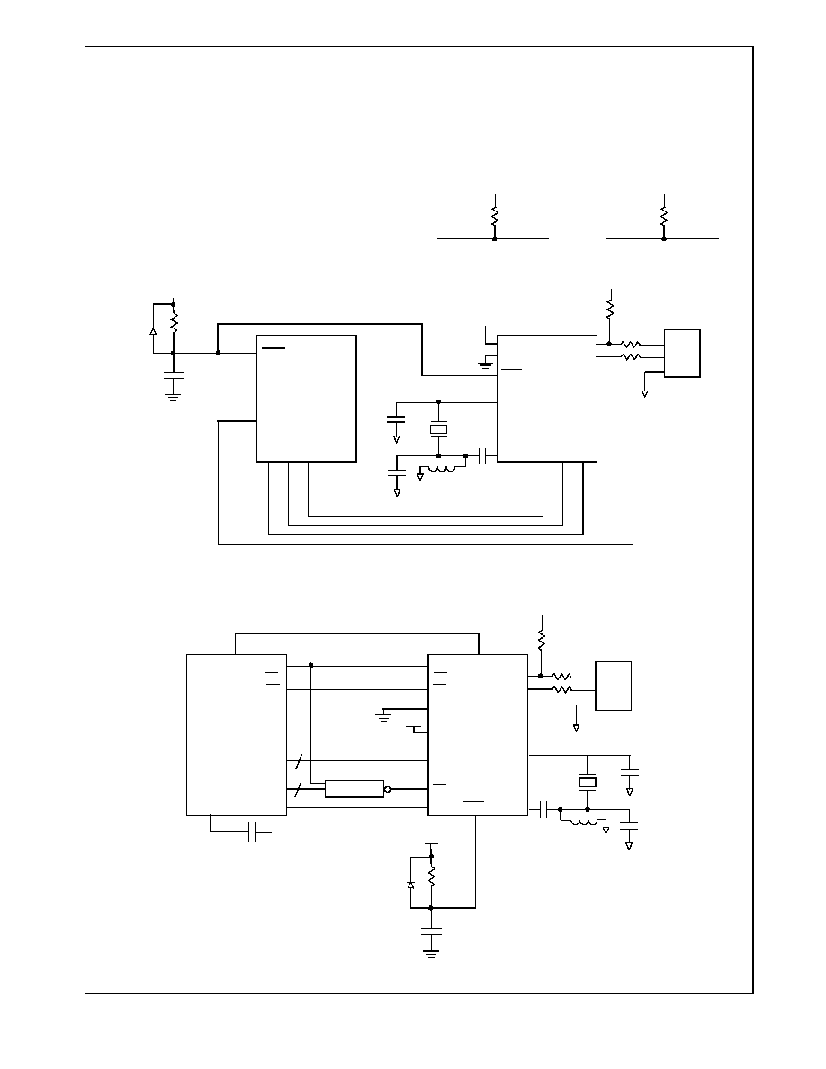
35
www.national.com
12.0 Design considerations
12.1 Targeted Applications
The USBN9602 is designed to be used in Full Speed USB
operations. The target applications are self-powered
devices like modems, printers, storage devices, imaging
devices, etc.
The USBN9602 is not intended for use in low speed appli-
cations. While not normally intended for bus-powered oper-
ation, this is possible in some cases with the addition of
external circuitry. Contact National Semiconductor for the
application notes that describe bus-powered use.
12.2 3.3V Regulator Issues
To comply with the Agreed USB Device Working Group
Review Requests - 110 dated July 7, 1997, a 7.5 k
�
1%
resistor can be tied from D+ to Vcc, or use a 1.13 k
�
1%
resistor tied to 3.3V.
D+
7.5 k
� 1%
Vcc = 5V
D+
1.13 k
�1%
Vcc = 3.3V
OR
12.3 Simplified Application Diagrams
COP888EG
10 uF
IN
RST
CKI
G0/INT
SL SO SK
3.3V
AGND
USB
D+
VCC
1.5K
4148
RST
INTR
CLKOUT
SK SI SO
D-
CONNECTOR
24
470nH
D+
D-
MODE1
MODE0
VCC
22 pF
56 pF
24
USBN9602
100 nF
10K
48 MHz
Figure 20. MICROWIRE Serial Interface
3rd
harmonic
XIN
XOUT
Note: pull all unused input and I/O pins up or down, as appropriate.
8051
10 uF
IN
XTAL1
ALE
3.3V
AGND
USB
D+
VCC
1.5K
4148
CS
D-
CONNECTOR
24
D+
D-
MODE1
MODE0
VCC
24
USBN9602
DECODER
10K
Figure 21. Multiplex Parallel Interface
WR
RD
AD7
AD0
A8 - A15
INTO
INTR
ALE
WR
RD
AD7
AD0
CLKOUT
8
8
RST
RESET
VCC
10 uF
470nH
22 pF
56 pF
100 nF
48 MHz
3rd
harmonic
XIN
XOUT

36
www.national.com
13.0 Memory Map
Table 8 is a memory map showing the addresses of the
USBN9602 registers.
Table 8. USBN9602 Memory Map
Address
Register
Name
Register
Function
0x00
MCNTRL
Main Control Register
0x01
CCONF
Clock Configuration Register
0x02
reserved
reserved
0x03
RID
Revision Identifier
0x04
FAR
Function Address Register
0x05
NFSR
Node Functional State Register
0x06
MAEV
Main Event Register
0x07
MAMSK
Main Mask Register
0x08
ALTEV
Alternate Event Register
0x09
ALTMSK
Alternate Mask Register
0x0A
TXEV
Transmit Event Register
0x0B
TXMSK
Transmit Mask Register
0x0C
RXEV
Receive Event Register
0x0D
RXMSK
Receive Mask Register
0x0E
NAKEV
NAK Event Register
0x0F
NAKMSK
NAK Mask Register
0x10
FWEV
FIFO Warning Event Register
0x11
FWMSK
FIFO Warning Mask Register
0x12
FNH
Frame Number Register High
Byte
0x13
FNL
Frame Number Register Low Byte
0x14
DMA
CNTRL
DMA Control Register
0x15-
0x1F
reserved
reserved
0x20
EPC0
Endpoint Control Register 0
0x21
TXD0
Transmit Data Register 0
0x22
TXS0
Transmit Status Register 0
0x23
TXC0
Transmit Command Register 0
0x24
reserved
reserved
0x25
RXD0
Receive Data Register 0
0x26
RXS0
Receive Status Register 0
0x27
RXC0
Receive Command Register 0
0x28
EPC1
Endpoint Control Register 1
0x29
TXD1
Transmit Data Register 1
0x2A
TXS1
Transmit Status Register 1
0x2B
TXC1
Transmit Command Register 1
0x2C
EPC2
Endpoint Control Register 2
0x2D
RXD1
Receive Data Register 1
0x2E
RXS1
Receive Status Register 1
0x2F
RXC1
Receive Command Register 1
0x30
EPC3
Endpoint Control Register 3
0x31
TXD2
Transmit Data Register 2
0x32
TXS2
Transmit Status Register 2
0x33
TXC2
Transmit Command Register 2
0x34
EPC4
Endpoint Control Register 4
0x35
RXD2
Receive Data Register 2
0x36
RXS2
Receive Status Register 2
0x37
RXC2
Receive Command Register 2
0x38
EPC5
Endpoint Control Register 5
0x39
TXD3
Transmit Data Register 3
0x3A
TXS3
Transmit Status Register 3
0x3B
TXC3
Transmit Command Register 3
0x3C
EPC6
Endpoint Control Register 6
0x3D
RXD3
Receive Data Register 3
0x3E
RXS3
Receive Status Register 3
0x3F
RXC3
Receive Command Register 3
Address
Register
Name
Register
Function

37
www.national.com
14.0 Electrical Characteristics
Absolute Maximum Ratings
Absolute Maximum Ratings indicate limits beyond which damage to the device may occur.
Supply Voltage
-0.5V to +7.0V
DC Input Voltage
-0.5V to Vcc +0.5V
DC Output Voltage
-0.5V to Vcc +0.5V
Storage Temperature
-65�C to +150�C
Lead Temperature (Soldering 10 seconds)
260�C
ESD Rating
1
1. Human body model; 100pF discharged through a 1.5 k
resistor.
2 kV
DC Electrical Characteristics
(4.5V< V
CC
< 5.5V
1
, 0
�
C < T
A
< +70
�
C, unless otherwise specified)
Symbol
Parameter
Condition
Min
Typ.
Max
Units
OPERATING RATINGS
I
cc1
Operating Supply Current
30
40
mA
I
cc2
Standby Supply Current
suspend mode: clock
off, no accesses.
5
10
mA
USB SIGNALS
V
DI
Differential Input Sensitivity
(D+) � (D�)
-0.2
0.2
V
V
CM
Differential Common Mode Range
0.8
2.5
V
V
SE
Single Ended Receiver Threshold
0.8
2.0
V
V
OL
Output Low Voltage
R
L
= 1.5k to 3.6V
0.3
V
V
OH
Output High Voltage
R
L
= 15k to GND
2.8
3.6
V
I
OZ
TRI-STATE Data Line Leakage
0V < V
IN
< 3.3V
-10
10
�
A
C
TRN
Transceiver Capacitance
20
pF
DIGITAL INPUTS/OUTPUTS (RESET, MODE, CLKOUT, AD0-AD7, WR, RD, A0)
V
OH
Output High Voltage
I
OH
= -6mA
2.4
V
V
OL
Output Low Voltage
I
OL
= 6mA
0.4
V
V
IH
Input High Voltage
2.0
V
V
IL
Input Low Voltage
0.8
V
I
IL
Input Low Current
V
IN
= GND
-10
�
A
I
IH
Input High Current
V
IN
= Vcc
10
�
A
I
OZ
TRI-STATE Leakage
2
V
OUT
= Vcc or GND
-10
10
�
A

38
www.national.com
14.0 Electrical Characteristics
(Continued)
OSCILLATOR INPUT/OUTPUT (XIN, XOUT)
V
IH
Input High Switching Level
3
4.5
V
V
IL
Input Low Switching Level
3
1.35
V
1. V
CC
should be between 4.75V and 5.25V if the internal 3.3V regulator is used. If external 3.3V regulator is
used, voltage on the V3.3 pin should be between 3.15 and 3.6V and V
CC
remains between 4.5V and 5.5V.
2. Not testable due to 15k pulldown resistor per USB Specification.
3. When XIN is used as an input for an external oscillator, the duy cycle must be between 45% and 55%.
AC Electrical Characteristics
(4.5V< V
CC
< 5.5V
1
, 0�C < T
A
< +70�C, unless otherwise specified)
1. V
CC
should be between 4.75V and 5.25V if the internal 3.3V regulator is used. If external 3.3V regulator is
used, voltage on the V3.3 pin should be between 3.15 and 3.6V and V
CC
remains between 4.5V and 5.5V.
Symbol
Parameter
Condition
2,3
2. Testing will be centered around 50
, not 45
� 15% as specified in USB Specification Revision 1.0.
3. Waveforms are measured from 10% to 90%.
Min
Typ
Max
Units
FULL SPEED SIGNALING (D+, D�)
T
R
Rise Time
C
L
= 50pF
4
20
nS
T
F
Fall Time
C
L
= 50pF
4
20
nS
T
RFM
Rise / Fall Time Matching (T
R
/T
F
)
C
L
= 50pF
90
110
%
V
CRS
Output Signal Crossover Voltage
4
4. Not testable.
C
L
= 50pF
1.3
2.0
V
Z
DRV
Driver Output Impedance (Single Ended)
C
L
= 50pF
5
5. Includes external resistor of 18
.
28
43
CLOCK OUT CHARACTERISTICS (CLKOUT)
T
R
Output Rise Time
C
L
=50pF
6
6. Fout<48 MHz.
15
nS
T
F
Output Fall Time
C
L
=50pF
6
15
nS
T
CYCLE
Output Duty Cycle
45
55
%
DC Electrical Characteristics
(4.5V< V
CC
< 5.5V
1
, 0
�
C < T
A
< +70
�
C, unless otherwise specified)
Symbol
Parameter
Condition
Min
Typ.
Max
Units

39
www.national.com
14.0 Electrical Characteristics
(Continued)
14.1 Parallel Interface Timing (MODE[1:0] = 00
b
)
INTERFACE TIMING (MODE = 0)
(4.5V< V
CC
< 5.5V, 0�C < T
A
< +70�C, unless otherwise specified)
Symbol
Parameter
Condition
Min
Typ
Max
Units
t
CS
Chip Select Setup Time
C
L
50pF
0
nS
t
CH
Chip Select Hold Time
C
L
50pF
5
nS
t
AS
Address Setup Time
C
L
50pF
0
nS
t
AH
Address Hold Time
C
L
50pF
0
nS
t
RW
Read Pulse Width
1
1. Clock Input: CKI = 48MHz on this device.
C
L
50pF
1/CKI
nS
t
RC
Read Cycle Time
2, 3
2. Memory Clock: MCLK = CKI/4 = 12 MHz.
3. Time until next Read or Write occurs.
C
L
50pF
3/MCLK
nS
t
RDV
Data output Valid after Read Low
C
L
50pF
20
30
nS
t
RDZ
Data output Hold after Read High
C
L
50pF
0
8
nS
t
WW
Write Pulse Width
1
C
L
50pF
1/CKI
nS
t
WC
Write Cycle Time
2,3
C
L
50pF
3/MCLK
nS
t
DS
Data input Setup Time
C
L
50pF
25
nS
t
DH
Data input Hold Time
C
L
50pF
5
nS
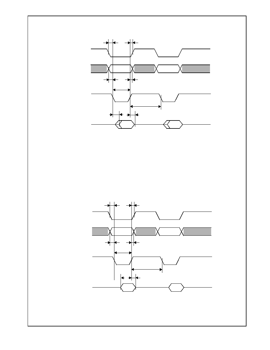
40
www.national.com
14.0 Electrical Characteristics
(Continued)
A0
CS
D[7:0] output
valid
valid
RD
t
AS
t
RDZ
t
RDV
t
RC
t
RW
t
CS
t
CH
t
AH
Consecutive Read Cycles Shown
Figure 22. Non-Multiplexed Mode Read Timing
A0
CS
D[7:0] input
valid
valid
WR
t
AS
t
DH
t
WC
t
WW
t
CS
t
CH
t
AH
Consecutive Write Cycles Shown
Figure 23. Non-Multiplexed Mode Write Timing
t
DS

41
www.national.com
14.0 Electrical Characteristics
(Continued)
14.2 Parallel Interface Timing (MODE[1:0] = 01
b
)
INTERFACE TIMING (MODE = 1)
(4.5V< V
CC
< 5.5V, 0�C < T
A
< +70�C, unless otherwise specified)
Symbol
Parameter
Condition
Min
Typ
Max
Units
t
AH
ALE High Time
1
1. Clock Input: CKI = 48 MHz on this device.
C
L
50pF
1/CKI
nS
t
CLAL
Chip Select Low to ALE Low
C
L
50pF
1/CKI
nS
t
AVAL
Address Valid to ALE Low
C
L
50pF
10
nS
t
AHAL
Address Hold after ALE Low
C
L
50pF
10
nS
t
ALRL
ALE Low to RD Low
2
2. Memory Clock: MCLK = CKI/4 = 12 MHz.
C
L
50pF
3/MCLK
nS
t
RLDV
Read Low to Data Valid
C
L
50pF
20
30
nS
t
RHDZ
Data Hold after Read High
C
L
50pF
0
8
nS
t
RL
Read Pulse Width
C
L
50pF
1/CKI
nS
t
WHAH
Write High to next ALE High
C
L
50pF
3/MCLK
nS
t
WHCH
Write High to CS High
C
L
50pF
10
nS
t
WL
Write Pulse Width
C
L
50pF
1/CKI
nS
t
DSWH
Data Setup to WR High
C
L
50pF
25
nS
t
DHWH
Data Hold after WR High
C
L
50pF
15
nS
ALE
CS
AD[7:0]
DATA
ADDR
RD
t
AH
t
CLAL
t
AVAL
t
ALRL
t
AHAL
t
RLDV
t
RHDZ
t
RL
Figure 24. Multiplexed Mode Interface Read Timing

42
www.national.com
14.0 Electrical Characteristics
(Continued)
ALE
CS
AD[7:0]
DATA
ADDR
WR
t
AH
t
CLAL
t
AVAL
t
WL
t
AHAL
t
DHWH
t
DSWH
t
WHCH
t
WHAH
Figure 25. Multiplexed Mode Interface Write Timing
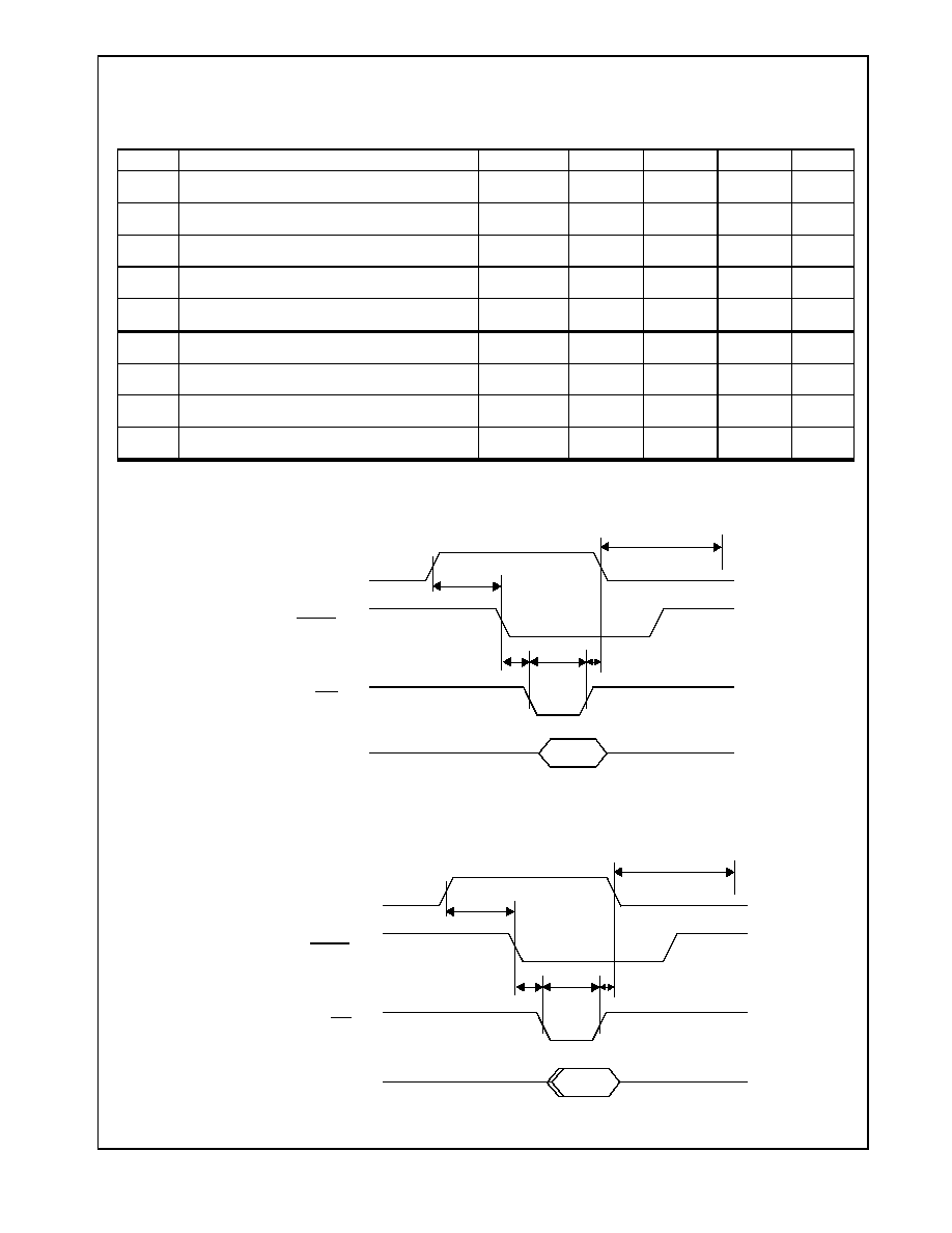
43
www.national.com
14.0 Electrical Characteristics
(Continued)
14.3 DMA Support Timing
.
.
DMA TIMING
(4.5V< V
CC
< 5.5V, 0�C < T
A
< +70�C, unless otherwise specified)
Symbol
Parameter
Condition
Min
Typ
Max
Units
t
RHAL
Request High to ACK Low
C
L
50pF
0
nS
t
ALWL
ACK low to Write Low
C
L
50pF
0
nS
t
WW
Write Pulse Width
C
L
50pF
1/CKI
nS
t
WRL
Write Low to Request Low
C
L
50pF
20
nS
t
DWR
DMA Write Recovery
1
1. Applicable if DMA transfer is not interrupted by read or write. If the transfer is interrupted, two additional
MCLK cycles are used.
C
L
50pF
2/MCLK
nS
t
ALRL
ACK low to Read Low
C
L
50pF
0
nS
t
RW
Read Pulse Width
C
L
50pF
1/CKI
nS
t
RRL
Read Low to Request Low
C
L
50pF
20
nS
t
DRR
DMA Read Recovery
1
C
L
50pF
2/MCLK
nS
DACK
DRQ
D[7:0]
WR
input
t
ALWL
t
RHAL
t
WW
t
WRL
t
DWR
Figure 26. DMA Write to USBN9602
DACK
DRQ
D[7:0]
RD
output
t
ALRL
t
RHAL
t
RW
t
RRL
t
DRR
Figure 27. DMA Read to USBN9602
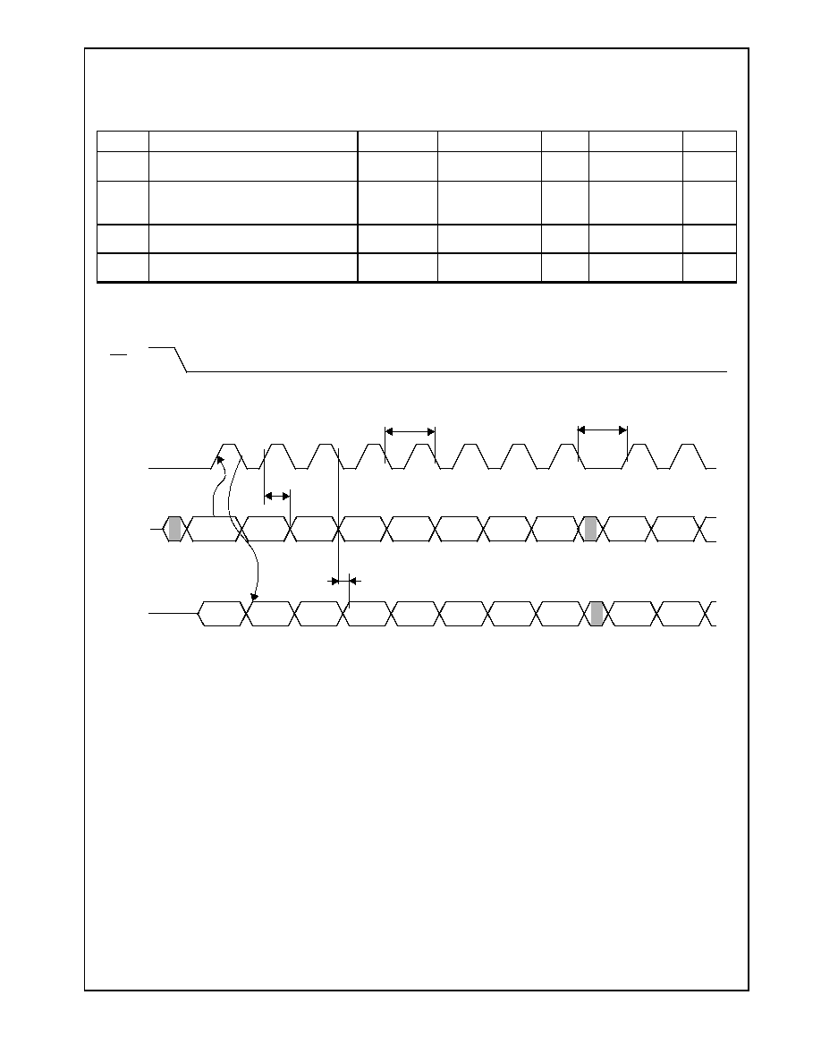
44
www.national.com
14.0 Electrical Characteristics
(Continued)
14.4 MICROWIRE Interface Timing (MODE[1:0] = 10
b
)
INTERFACE TIMING (MODE = 2)
(4.5V< V
CC
< 5.5V, 0�C < T
A
< +70�C, unless otherwise specified)
Symbol
Parameter
Condition
Min
Typ
Max
Units
t
SKC
SK Cycle Time
1
1. Memory Clock: MCLK = CKI/4 = 12 MHz.
C
L
50pF
4/MCLK
nS
t
CC
Time between two consecutive
8 clock cycles
1
C
L
50pF
4/MCLK
nS
t
SIH
Serial Input Hold Time
C
L
50pF
3/MCLK
nS
t
SOV
Serial Output Valid Time
C
L
50pF
3/MCLK
nS
SI
CS
6
5
4
3
2
1
LSB
MSB
6
SK
SO
6
5
4
3
2
1
LSB
6
MSB
t
SOV
t
SIH
t
SKC
t
CC
MSB
MSB
NOTE: The first eight SK cycles shift out the current contents of the shift register.
Figure 28. MICROWIRE Interface Timing
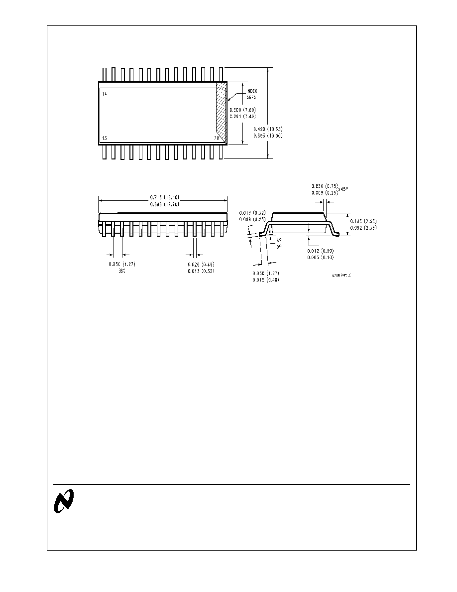
National does not assume any responsibility for use of any circuitry described, no circuit patent licenses are implied and National reserves the right at any time without notice to change said circuitry and specifications.
U
S
B
N
9
6
0
2
(
U
n
i
v
e
r
s
a
l
S
e
r
i
a
l
B
u
s
)
F
u
l
l
S
p
e
e
d
F
u
n
c
t
i
o
n
C
o
n
t
r
o
l
l
e
r
W
i
t
h
D
M
A
S
u
p
p
o
r
t
LIFE SUPPORT POLICY
NATIONAL'S PRODUCTS ARE NOT AUTHORIZED FOR USE AS CRITICAL COMPONENTS IN LIFE SUPPORT
DEVICES OR SYSTEMS WITHOUT THE EXPRESS WRITTEN APPROVAL OF THE PRESIDENT OF NATIONAL
SEMICONDUCTOR CORPORATION. As used herein:
1. Life support devices or systems are devices or systems
which, (a) are intended for surgical implant into the body,
or (b) support or sustain life, and whose failure to per-
form, when properly used in accordance with instructions
for use provided in the labeling, can be reasonably ex-
pected to result in a significant injury to the user.
2. A critical component is any component of a life support
device or system whose failure to perform can be rea-
sonably expected to cause the failure of the life support
device or system, or to affect its safety or effectiveness.
National Semiconductor
Corporation
Tel: 1-800-272-9959
Fax: 1-800-737-7018
Email: support@nsc.com
National Semiconductor
Europe
Fax:
(+49) 0-180-530 85 86
Email:
europe.support@nsc.com
Deutsch Tel:
(+49) 0-180-530 85 85
English Tel:
(+49) 0-180-532 78 32
National Semiconductor
Japan Ltd.
Tel: 81-3-5620-6175
Fax: 81-3-5620-6179
National Semiconductor
Asia Pacific
Customer Response Group
Tel: 65-254-4466
Fax: 65-250-4466
Email: sea.support@nsc.com
www.national.com
15.0 Physical Dimensions
inches (millimeters) unless otherwise noted
Molded SO Wide Body Package (WM)
Order Number USBN9602-28M
See NS Package Number M28B