NTE7039 & NTE7104
Integrated Circuit
Vertical Deflection Output Circuit
w
/Drive Circuit for CRT Display
Description:
The NTE7039 and NTE7104 are vertical deflection output ICs developed for use in high≠grade TVs
and displays. The interlace and crossover distortion responses, in particular, have been greatly im-
proved, allowing excellent picture quality on large size television screens and high precision interlace
mode displays.
Also, pulse signals can be used for input signals due to the on≠chip sawtooth wave generating circuit
and driver circuit. Further, the DC and AC feedback circuits can be formed with these ICs alone, sim-
plyfing pattern design of sets and ensuring stable performance.
The NTE7104 has a maximum deflection current of 1.8A
p≠p
, making it appropriate for use in portable
to mid≠size televisions while the NTE7039 has a minimum deflection current of 2.2A
p≠p
, so it can be
used for larger size sets, and can drive television screen sizes from 33 to 37 inches.
Features:
D
Low Power Dissipation due to On≠Chip Pump≠Up Circuit
D
On≠Chip 50/60Hz Vertical Size Control Circuit
D
On≠Chip Sawtooth Wave Generating Circuit
D
On≠Chip Drive Circuit
D
Vertical Output Circuit
D
On≠Chip Thermal Protection Circuit
D
Excellent Interlace Response
D
Excellent Crossover Response
Absolute Maximum Ratings: (T
A
= +25
∞
C unless otherwise specified)
Driver Supply Voltage, +V
CC
1 max
15V
. . . . . . . . . . . . . . . . . . . . . . . . . . . . . . . . . . . . . . . . . . . . . . . . . . .
Pump≠Up Supply Voltage, +V
CC
8 max
30V
. . . . . . . . . . . . . . . . . . . . . . . . . . . . . . . . . . . . . . . . . . . . . . . .
Output Supply Voltage, +V
CC
13 max
62V
. . . . . . . . . . . . . . . . . . . . . . . . . . . . . . . . . . . . . . . . . . . . . . . . . .
Deflection Output Current, I
DEF
≠1.5 to +1.5A
P≠O
. . . . . . . . . . . . . . . . . . . . . . . . . . . . . . . . . . . . . . . . . .
Thermal Resistance, Junction≠to≠Case, R
thJ≠C
4
∞
C/W
. . . . . . . . . . . . . . . . . . . . . . . . . . . . . . . . . . . . . .
Allowable Power Dissipation (With Infinite Heat Sink), P
D
max
8W
. . . . . . . . . . . . . . . . . . . . . . . . . . .
Operating Temperature Range, T
opr
≠20
∞
to +85
∞
C
. . . . . . . . . . . . . . . . . . . . . . . . . . . . . . . . . . . . . . . . .
Storage Temperature Range, T
stg
≠40
∞
to +150
∞
C
. . . . . . . . . . . . . . . . . . . . . . . . . . . . . . . . . . . . . . . . . .
Recommended Operating Conditions: (T
A
= +25
∞
C unless otherwise specified)
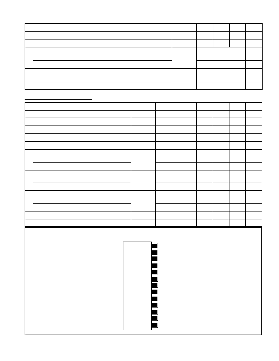
Parameter
Symbol
Min
Typ
Max
Unit
Driver Supply Voltage
+V
CC
1
8
12
14
V
Pump≠Up Supply Voltage
+V
CC
8
10
24
27
V
Deflection Output Current
NTE7039
I
12p≠p
up to 2.2
A
p≠p
NTE7104
up to 1.8
A
p≠p
Ramp Waveform Pulse Height
NTE7039
V
6p≠p
up to +B1/3
V
p≠p
NTE7104
up to ≠1.01
V
p≠p
Electrical Characteristics: (T
A
= +25
∞
C, +V
CC
1 = 12V, +V
CC
8 = 24V unless otherwise specified)
Parameter
Symbol
Test Conditions
Min
Typ
Max
Unit
Driver Supply Current
I
CC
1
5.6
6.7
7.8
mA
Trigger Input Threshold Voltage
V
2
2.6
2.9
3.2
V
Vertical Amplitude Control Pin Voltage
V
4
5.9
6.1
6.3
V
Ramp Waveform Generator Start Voltage
V
RAMP
4.6
4.9
5.2
V
Pump≠Up Charge Saturation Voltage
V
S9≠11
I
9
= 20mA
≠
≠
1.8
V
Pump≠Up Discharge Saturation Voltage
NTE7039
V
S8≠9
I = 1.1A
≠
≠
3.2
V
NTE7104
I = 0.9A
≠
≠
3.0
V
Deflection Output Saturation Voltage (Lower)
NTE7039
V
S12≠11
I = 1.1A
≠
≠
1.5
V
NTE7104
I = 0.9A
≠
≠
1.2
V
Deflection Output Saturation Voltage (Upper)
NTE7039
V
S13≠12
I = 1.1A
≠
≠
3.5
V
NTE7104
I = 0.9A
≠
≠
3.2
V
Idling Current
I
DL
35
≠
65
mA
Voltage Gain
≠
59
≠
dB
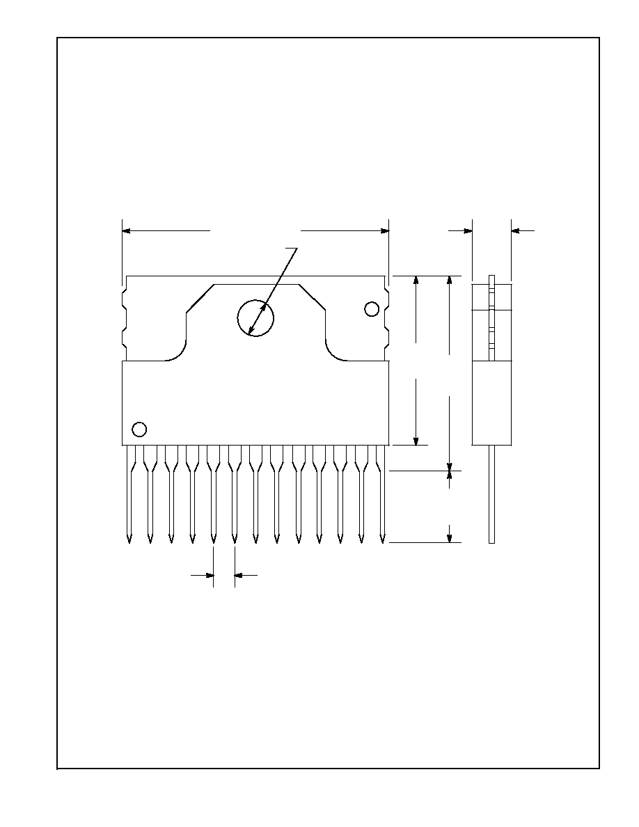
Pin Connection Diagram
+V
CC
8
+V
CC
1
Vertical Trigger Input
Time Constant
Vertical Output
OSC Stop
Power Supply for
Vertical Size Control
Vertical Output
Pump≠Up Output
Vertical Amp Control
GND
13
12
11
10
9
8
7
Ramp Generator
6
5
4
3
2
1
AC/DC Feedback
Vertical Output
(Front View)