 | –≠–ª–µ–∫—Ç—Ä–æ–Ω–Ω—ã–π –∫–æ–º–ø–æ–Ω–µ–Ω—Ç: NTE1570 | –°–∫–∞—á–∞—Ç—å:  PDF PDF  ZIP ZIP |

NTE1570 (NPN Tuner) & NTE1572 (FET Tuner)
Integrated Circuit
TV Video IF, Sound IF
Functions:
PIF
D
Three Controlled IF Amplifier Stages
D
Video Demodulator Controlled by Picture Carrier
D
Black Noise and White Noise Inverter
D
Peak AGC
D
DC Amplifier for RF AGC Out
SIF
D
Three Differential IF Amplifier Stages
D
Phase Detector
D
DC Controlled Attenuator
D
Audio Amplifier Stage with NFB Terminal
Features:
D
PIF, SIF, ATT Audio Driver
D
2 Chip Color TV System is Possible with NTE1547
PIF
D
High Gain, Wide Band IF Amplifier
D
AGC Characteristics with Excellent Stability
D
Excellent DG/DP Characteristics
D
Excellent S/N Chracteristics due to Delayed 3
Stage AGC Action
D
Negative Video Output Signal
D
Switch Off the Video Part with VTR Switch
SIF
D
Excellent Limiter Charactristics
D
Excellent Attenuato Characteristics
Absolute Maximum Ratings: (T
A
= +25
∞
C unless otherwise specified)
Supply Voltage, V
CC
15V
. . . . . . . . . . . . . . . . . . . . . . . . . . . . . . . . . . . . . . . . . . . . . . . . . . . . . . . . . . . . . . . .
Pin11 Open Voltage, V
11
15V
. . . . . . . . . . . . . . . . . . . . . . . . . . . . . . . . . . . . . . . . . . . . . . . . . . . . . . . . . . . .
Video DC Output Current, I
15
6mA
. . . . . . . . . . . . . . . . . . . . . . . . . . . . . . . . . . . . . . . . . . . . . . . . . . . . . . .
Audio DC Output Current, I
3
3mA
. . . . . . . . . . . . . . . . . . . . . . . . . . . . . . . . . . . . . . . . . . . . . . . . . . . . . . . .
Pin2 Voltage, V
2
15V
. . . . . . . . . . . . . . . . . . . . . . . . . . . . . . . . . . . . . . . . . . . . . . . . . . . . . . . . . . . . . . . . . . .
Power Dissipation, P
D
1.6W
. . . . . . . . . . . . . . . . . . . . . . . . . . . . . . . . . . . . . . . . . . . . . . . . . . . . . . . . . . . . .
Derate Above 25
∞
C
12.8mW/
∞
C
. . . . . . . . . . . . . . . . . . . . . . . . . . . . . . . . . . . . . . . . . . . . . . . . . . . .
Operating Temperature Range, T
opr
≠20
∞
to +65
∞
C
. . . . . . . . . . . . . . . . . . . . . . . . . . . . . . . . . . . . . . . . .
Storage Temperature range, T
stg
≠55
∞
to +150
∞
C
. . . . . . . . . . . . . . . . . . . . . . . . . . . . . . . . . . . . . . . . . . .
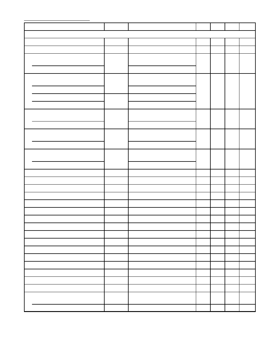
Electrical Characteristics: (T
A
= +25
∞
C, V
CC
= 12V, f
p
= 58.75MHz, f
S
= 54.25MHz)
Parameter
Symbol
Test Conditions
Min
Typ
Max
Unit
PIF Section
Recommended Supply Voltage
V
CC
10.8
12.0
13.2
V
Supply Current
I
CC
50
72
95
mA
Video DC Output Voltage
NTE1570
V
15
SW
1
: 2, SW
2
: 2
5.2
5.5
5.8
V
NTE1572
SW
1
: 1, SW
2
: 2
AFT DC Output Voltage
NTE1570
V
13
SW
1
: 2, SW
2
: 2
5.3
6.8
8.3
V
NTE1572
SW
1
: 1, SW
2
: 2
NTE1570
V
14
SW
1
: 2, SW
2
: 2
NTE1572
SW
1
: 1, SW
2
: 2
AFT DC Offset Voltage
NTE1570
V
13≠14
SW
1
: 2, SW
2
: 2
≠1.5
0
+1.5
V
NTE1572
SW
1
: 1, SW
2
: 2
RF AGC Residual Output Voltage
NTE1570
V
11(sat)
SW
1
: 2, SW
2
: 2
≠
≠
0.5
V
NTE1572
SW
1
: 1, SW
2
: 2
RF AGC Leakage Current
NTE1570
I
11(leak)
SW
1
: 2, SW
2
: 1
≠
≠
1.0
µ
A
NTE1572
SW
1
: 1, SW
2
: 1
Video Sensitivity (Pin7≠Pin8)
v
i
Note 1
60
150
250
µ
V
rms
AGC Range
A
PIF
Note 2
60
64
≠
dB
Sync Tip Level Voltage (V
15
)
V
SYNC
Note 3
2.3
2.5
2.7
V
Maximum IF Input Voltage (PIF)
i
IN(MAX)
Note 4
100
120
≠
mV
rms
White Noise Threshold Level (V
15
)
V
WTH
Note 5
5.8
6.2
6.6
V
White Noise Clamp Level (V
15
)
V
WCL
Note 5
3.7
4.1
4.5
V
Black Noise Threshold Voltage (V
15
)
V
BTH
Note 5
1.4
1.6
1.8
V
Black Noise Clamp Level (V
15
)
V
BCL
Note 5
2.9
3.3
3.7
V
Video Frequency Response
f
BW
Note 6
4.5
5.5
≠
MHz
Suppression of Carrier
CL
Note 7
40
50
≠
dB
Suppression of 2
nd
Carrier
I
2nd
Note 8
40
50
≠
dB
920kHz Beat Level
I
920
Note 9
33
38
≠
dB
Differential Phase
DP
Note 10
≠
3.5
5.0
deg
Differential Gain
DG
Note 10
≠
7
10
%
PIF Input Impedance
R
IN(PIF)
Note 11
1.5
3.0
6.0
k
PIF Input Capacitance
C
IN(PIF)
Note 11
≠
3
10
pF
AFT Output Voltage
Upper
V
13U
, V
14U
Note 13
11.7
11.9
12.0
V
Lower
V
13L
, V
14L
1.8
2.3
2.8
V
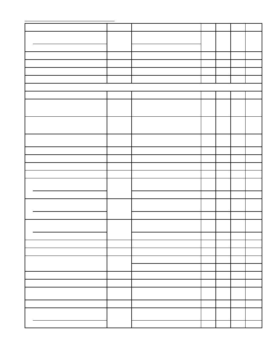
Electrical Characteristics (Cont'd): (T
A
= +25
∞
C, V
CC
= 12V, f
p
= 58.75MHz, f
S
= 54.25MHz)
Parameter
Symbol
Test Conditions
Min
Typ
Max
Unit
RF AGC Maximum Available Current
NTE1570
I
4(max)
SW
1
: 2, SW
2
: 1
7.0
≠
≠
mA
NTE1572
SW
1
: 1, SW
2
: 1
0.3
≠
≠
mA
RF AGC Delay Setting Range (Delay)
V
IN
Note 14
5
7
9
V
AFT Band Width
F
W
Note 13
1.4
≠
≠
MHz
Video Output Voltage
v
OUT
Note 15
2.25
2.50
2.75
V
SIF Output Voltage
S
OUT
Note 16
200
400
600
mV
rms
SIF Section
Input Limiting Voltage
v
IN(LIM)
R
D
=
, Note 17
≠
200
400
µ
V
rms
AM Rejection Ratio
AMR
SIF IN: f = 4.5MHz, f
m
= 400Hz,
f =
±
25kHz, AM: 30%,
v
in
= 100dB
µ
40
45
≠
dB
Recovered Output Voltage
V
OD
SIF IN: f = 4.5MHz, f
m
= 400Hz,
f =
±
25kHz, v
in
= 80dB
µ
,
R
D
= 12k
0.5
0.75
≠
V
rms
Total Harmonic Distortion
THD
SIF IN: f = 4.5MHz, f
m
= 400Hz,
f =
±
25kHz, v
in
= 80dB
µ
≠
1.0
≠
%
Max. Audio Output Voltage
v
OM
SIF IN: f = 4.4 to 4.6MHz
4.0
≠
≠
V
P≠P
SIF Input Impedance
R
IN(SIF)
f = 4.5MHz
10
20
30
k
SIF Input Capacitance
C
IN(SIF)
f = 4.5MHz
≠
3.0
≠
pF
DET Output Impedance
R
O(DET)
Note 18
10
15
20
k
DC Voltage, Pin21
NTE1570
V
21
SW
1
: 2, SW
2
: 2
3.5
4.4
5.3
V
NTE1572
SW
1
: 1, SW
2
: 2
3.5
4.4
5.3
V
DC Voltage, Pin23
NTE1570
V
23
SW
1
: 2, SW
2
: 2
4.8
6.0
7.2
V
NTE1572
SW
1
: 1, SW
2
: 2
4.8
6.0
7.2
V
DC Voltage, Pin1
NTE1570
V
1
SW
1
: 2, SW
2
: 2
6.0
6.7
7.4
V
NTE1572
SW
1
: 1, SW
2
: 2
6.0
6.7
7.4
V
Max. Attenuation
ATT MAX
Note 19
60
≠
≠
dB
DC Volume Gain
G
ATT
MAX R
A
= 0
4
6
8
dB
ATT Characteristics
V
1
Note 22
3.4
3.8
4.2
V
Note 23
4.5
4.9
5.3
V
Signal Leakage
v
PT
Note 20
≠
1.0
3.0
mV
rms
AF Amp Gain
G
V
AF
Note 21
≠
20
≠
dB
AF Amp Distortion
THD AF
P
23A
= 1V
PP
, 400Hz, SW
3
: ON,
ATT: ≠26dB Setting
≠
1.5
≠
%
AF Amp Max. Output Voltage
v
OAF
MAX
THD
AF
= 5%, Note 21
1.5
2.0
≠
V
rms
AF Output DC Voltage
NTE1570
V
3
SW
1
: 2, SW
2
: 2
6.7
7.7
8.8
V
NTE1572
SW
1
: 1, SW
2
: 2
6.7
7.7
8.8
V

Notes:
Note 1. V
AGC
(P5 EXT. Applying Voltage) = 11.5V, PIF IN: f = 58.75MHz 1kHz 30% AM Modulation.
Adjust PIF input level (v
i
) so that the detected output of P
15A
with high impedance probe will
be 0.8V
P≠P
and measure the input level.
Note 2. V
AGC
= 4V. Measure PIF input level (v
i
) same as Note 1.
Note 3. PIF IN: f = 58.75MHz CW 15mV
rms
. Measure DC level of P
15
.
Note 4. PIF IN: f = 58.75MHz, APL 100%, 87.5% AM modulation. P
5
: Ppen.
(1) Adjust PIF input level 50mV
P≠P
and measure the detected output level v
01P≠P
.
(2) Then increase the input level so that the detected output level will be 1.1 x v
01P≠P
and measure the input level.
Note 5. V
AGC
= 8V. PIF IN: 58.75MHz
±
10MHz variable or sweep 15mV
rms
measure DC level of
P
15
.
Note 6. V
AGC
= 8V (GR = 30dB). SG
1
: 58.75MHz CW, SG
2
: 58.65 to 40MHz variable.
(1) Setting output of SG
1
so that DC level of P
15
will be 4V.
(2) Setting output of SG
2
(58.65MHz) so that AC level of P
15
will be 0.5V
P≠P
.
(3) Decreaseing frequency of SG
2
until AC level of P
15
will be 0.35V
P≠P
(≠3dB of 0.5V
P≠P
) then read f
SG2
= F, f
BW
= 58.75≠F MHz
Note 7. SG
1:
58.75MHz, 1kHz 80% AM modulation 100mV
rms
. SG
2
, SG
3
: OFF. Setting V
AGC
so
that output AC level of P
15
will be 2.7V
P≠P
. Measure CL of P
15
after setting to 0% AM of SG
1
.
Note 8. Measure I
2nd
of P
15
same as Note 7.
Note 9. V
AGC
= 8V. SG
1
: 58.75MHz (P = Picture) 100mV
rms
. SG
2
: 54.25MHz (S = Sound)
32mV
rms
(≠10dB of SG
1
). SG
3
: 55.17MHz (C = Chroma) 32mV
rms
(≠10dB of SG
1
).
(1) Seting V
AGC
so that the output tip level (lower) of P
15
will be 3V DC.
(2) Measure the level difference (dB) between c≠level and 920kHz level.
Note10. V
AGC
= 8V. PIF IN: f = 58.75MHz video signal (ramp) 87,5% AM 100mV
P≠P
. Setting ATT
so that the sync tip level of P
15
will be 2.5V DC. Measure DP and DG.
Note 11. V
AGC
= 5V, f = 58.75MHz. Measure R
IN
, C
IN
.
Note12. AFT sensitivity
F/
(V
13
≠V
14
)
(1) INT, AGC (P
5
Open)
(2) PIF Input: 58.75MHz
±
1MHz, CW 15mV
rms
.
(3) Read the frequency (f
1
) of PIF when V
13
≠V
14
= ≠1V.
(4) Read the frequency (f
2
) of PIF when V
13
≠V
14
= 1V.
Then calculate
F/
(V
13
≠V
14
) = |f
1
≠f
2
|
Note13.
F
W
, V
13U
, V
14U
, V
13L
, V
14L
(1) INT AGC (P
5
Open)
(2) PIF IN: 58.75MHz
±
10MHz CW 15mV
rms
(3) 9pF at Pin16 should b shorted
(4) Read the frequency (f
1
or f
2
) when the V
5
or V
6
reduced to 90% level of A or B with
varing the frequency. Then band width is the difference from center requency (f
0
).
Note14. P
5
: Open. PIF IN: 58.75MHz CW 20mV
rms
.
(1) Adjust the voltage of Pin3 so that the voltage of Pin4 will be 6V DC.
(2) Measure the volatge at Pin3.
Note15. P
5
: Open. PIF IN: 58.75MHz, 100% APL 87.5% AM modulation signal amplitude 50mV
P≠P
.
Measure detected output voltge (White peak to sync tip).
Note16. P
5
: Open. SG
1
: 58.75MHz CW 100mV
rms
. SG
2
: 54.25MHz CW 25mV
rms
. Measure SIF
(4.5MHz) output voltage at P
15
.
Note17. SIF IN: f = 4.5MHz, FM f
MOD
= 400Hz,
f =
±
25kHz.
(1) Adjust SIF input level 100mV
P≠P
and measure the detected output level v
OS
.
(2) Then decrease the input level so that the detected output level will be 3dB down of
v
OS
and measure the input level.

Notes (cont'd):
Note18. Output Impedance
(1) SIF IN: f = 4.5MHz, FM f
MOD
= 400Hz,
f =
±
25kHz, 80dB
µ
.
(2) At P
23
read the V
O1
at R
X
=
, then read the R
X
when recovered output become
V
O1
/2 with varying the R
X
. The R
X
is the output impedance.
Note19. ATT MAX.
(1) SIF IN: f = 4.5MHz, FM f
MOD
= 400Hz,
f =
±
25kHz, 80dB
µ
.
(2)
Read the 400Hz component of V
A1
at P
2
with R
A
= 0, then read V
A1'
with R
A
=
.
Note20. v
PT
(1) SIF IN: f = 4.5MHz, FM f
MOD
= 400Hz,
f =
±
25kHz, 80dB
µ
.
(2) Read the 400Hz component at P
3
.
Note21. G
V
AF
(1) Apply 400Hz 0.1V
rms
signal to P
2
.
(2) Read the output voltage at P
3
.
Note22. Read the 400Hz component of V
A1
at P
2
with R
A
= 0. Set R
A
so that V
A1'
= 1/2V
A1
(≠6dB),
then read DC voltage of Pin1 (V
1
).
Note23. Read the 400Hz component of V
A1
at P
2
with R
A
= 0. Set R
A
so that V
A1'
= 3.16 x 10
≠3
V
A1
(≠50dB), then read DC voltage of Pin1 (V
1
).
V
CC
Pin Connection Diagram
AFT Output 2
AFT Tank
Video Tank
SIF Detector
Video Tank
1
2
3
4
Volume Control
NFB
Audio Output
Audio GND
5
IF AGC Filter/
6
PIF Input
7
PIF Input
8
PIF Input
24
23
22
21
De≠Emphasis
SIF Detector
SIF Input
20
19
AFT Tank
18
17
9
PIF Input
16
Video Output
10
RF AGC Delay
11
RF AGC Output
15
14
AFT Output 1
12
PIF GND
13
VCR Switch
1
12
24
13
1.300 (33.02)
Max
.520
(13.2)
.600
(15.24)
1.100 (27.94)
.100 (2.54)
.225
(5.73)
Max
.126
(3.22)
Min