
NTE1633
Integrated Circuit
TV Sound Channel
w
/DC Controls
Description:
The NTE1633 is a complete TV sound channel in a 20≠Lead DIP type package with DC tone and vol-
ume controls plus separate VCR input and output connections. Supplied in a 20≠pin DIP, the device
delivers an output power of 4W into 16
(d = 10%, V
S
= 24V) or 1.5W into 8
(d = 10%, V
S
= 12V).
Included in the NTE1633 are: IF amplifier limiter, active low≠pass filter, AF preamplifier and power
amplifier, turnoff muting, mute circuit and thermal protection.
High output, high sensitivity, excellent AM rejection and low distortion make the device suitable for
use in TVs of almost any type. Further, no screening is necessary because the device is free of radi-
ation problems.
Features:
D
Separate VCR Input and Output Pins
D
4W Output Power into 16
D
No Screening Required
D
High Sensitivity
D
Excellent AM Rejection
D
Low Distortion
D
DC Tone/Volume Controls
D
Thermal Protection
Absolute Maximum Ratings:
Supply Voltage (Pin18), V
S
28V
. . . . . . . . . . . . . . . . . . . . . . . . . . . . . . . . . . . . . . . . . . . . . . . . . . . . . . . . . .
Voltage at Pin1, V
i
±
V
S
. . . . . . . . . . . . . . . . . . . . . . . . . . . . . . . . . . . . . . . . . . . . . . . . . . . . . . . . . . . . . . . . . .
Input Voltage (Pin2), V
i
1V
pp
. . . . . . . . . . . . . . . . . . . . . . . . . . . . . . . . . . . . . . . . . . . . . . . . . . . . . . . . . . . . .
Output Peak Current, I
O
Repetitive
1.5A
. . . . . . . . . . . . . . . . . . . . . . . . . . . . . . . . . . . . . . . . . . . . . . . . . . . . . . . . . . . . . . . . . .
Non≠Repetitive
2A
. . . . . . . . . . . . . . . . . . . . . . . . . . . . . . . . . . . . . . . . . . . . . . . . . . . . . . . . . . . . . . .
Current (Pin4), I
4
10mA
. . . . . . . . . . . . . . . . . . . . . . . . . . . . . . . . . . . . . . . . . . . . . . . . . . . . . . . . . . . . . . . . .
Power Dissipation (T
pins
= +90
∞
C), P
tot
4.3W
. . . . . . . . . . . . . . . . . . . . . . . . . . . . . . . . . . . . . . . . . . . . . . .
Power Dissipation (T
A
= +70
∞
C), P
tot
1.0W
. . . . . . . . . . . . . . . . . . . . . . . . . . . . . . . . . . . . . . . . . . . . . . . . .
Operating Junction Temperature Range, T
J
≠40
∞
to 150
∞
C
. . . . . . . . . . . . . . . . . . . . . . . . . . . . . . . . . . .
Storage Temperature Range, T
stg
≠40
∞
to 150
∞
C
. . . . . . . . . . . . . . . . . . . . . . . . . . . . . . . . . . . . . . . . . . .
Maximum Thermal Resistance, Junction≠to≠Pins, R
thJPins
14
∞
C/W
. . . . . . . . . . . . . . . . . . . . . . . . . . . .
Maximum Thermal Resistance, Junction≠to≠Ambient (Note 1), R
thJA
80
∞
C/W
. . . . . . . . . . . . . . . . . .
Note 1. Obtained with GND pins soldered to printed circuit with minimized copper area.
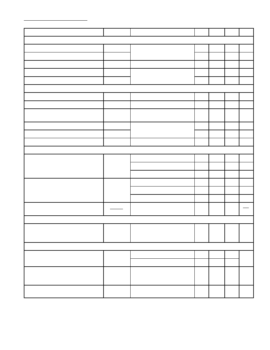
Electrical Characteristics: V
S
= 24V, S1: ON,
f =
±
25kHz, V
i
= 1mV, P
1
= 12k
, f
o
= 4.5MHz,
f
m
= 400Hz, T
A
= +25
∞
C unless otherwise indicated)
Parameter
Symbol
Test Conditions
Min
Typ
Max
Unit
DC Characteristics
Supply Voltage (Pin18)
V
S
P
2
= 12k
10.8
≠
27
V
Quiescent Output Voltage (Pin18)
V
O
11
12
13
V
DC Voltage (Pin1)
V
1
P
2
= 12k
, R
1
= 270k
≠
5.3
≠
V
DC Voltage (Pin4)
V
4
P
2
= 12k
≠
3.2
≠
V
Quiescent Drain Current (Pin4)
I
d
≠
32
≠
mA
IF Amplifier & Detector
Input Limiting Voltage @ Pin2 (≠3dB) V
i(threshold)
V
O
= 4V
rms
≠
50
100
µ
V
Recovered Audio Voltage (Pin9)
V
9
f =
±
7.5kHz, P
2
= 12k
140
200
280
mV
Amplitude Modulation Rejection
AMR
m = 0.3, V
1
= 1mV,
V
O
= 4V
rms
, Note 2
≠
60
≠
dB
Input Resistance (Pin2)
R
i
f = 0, P
2
= 12k
≠
30
≠
k
Input Capacitance (Pin2)
C
i
≠
6
≠
pF
De≠Emphasis Resistance
R9
C
1
= 60 to 888nF
0.75
1.1
1.5
k
DC Volume Control
Volume Attenuation
K
V
P
2
= 0
≠
0
≠
dB
(Resistance Control)
P
2
= 4.3k
20
26
32
dB
P
2
= 12k
≠
88
≠
dB
Control Voltage
V
C
K = 0dB
≠
0
≠
V
K = 26dB
≠
1.3
≠
V
K = 88dB
≠
2.6
≠
V
Volume Attenuation Thermal Drift
(Resistance Control)
K
V
T
pins
T
pins
= +25
∞
to +85
∞
C,
P
2
= 4.3k
≠
≠0.05
≠
dB
∞
C
DC Tone Control
Tone Cut
K
T
S1: OFF, V
10
= 200mV,
P
1
= 12k
to 100k
,
f
AF
= 10kHz
≠
14
≠
dB
Audio Frequency Amplifier
Output Power (d = 10%)
P
O
V
S
= 24V, R
L
= 16
3.5
4.1
≠
W
V
S
= 12V, R
L
= 8
≠
1.5
≠
Frequency Response of Audio
Amplifier (≠3dB)
B
P
O
= 1W, R
L
= 16
,
S1: OFF, V
10
= 200mV
V
O
= 4V
rms
, @ 400Hz
15
50
≠
kHz
Supply Voltage Rejection
SVR
P
2
= 12k
,
f =0,
f
ripple
= 120Hz
≠
26
≠
dB
Note 2. Test Bandwidth = 20kHz
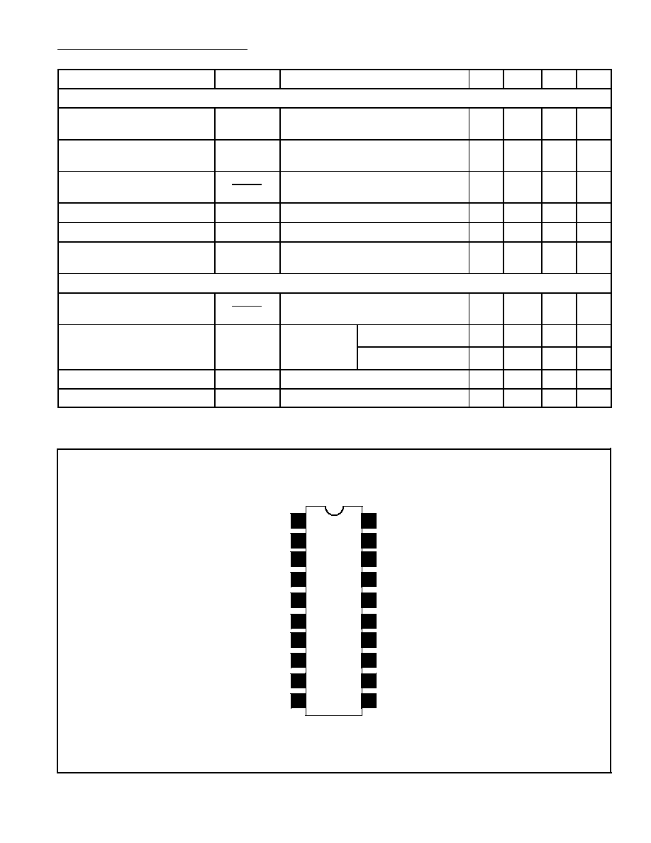
Electrical Characteristics (Cont'd): V
S
= 24V, S1: ON,
f =
±
25kHz, V
i
= 1mV, P
1
= 12k
,
f
o
= 4.5MHz, f
m
= 400Hz, T
A
= +25
∞
C unless otherwise indicated)
Parameter
Symbol
Test Conditions
Min
Typ
Max
Unit
VCR
Total Harmonic Distortion of
Pin9 Output Signal
d
f =
±
7.5kHz, V
i
= 1mV
≠
0.5
≠
%
Supply Voltage Rejection at
Output Pin9
SVR
f = 0, f
ripple
= 120Hz, P
2
= 12k
≠
66
≠
dB
Signal≠to≠Noise Ratio at
Output Pin9
S + N
N
f =
±
25kHz, V
I
1mV
≠
70
≠
dB
Input Voltage (Playback)
V
10
V
o
= 4V
rms
, P
2
= 0, S1: OFF
50
70
100
mV
Input Resistance (Playback)
R
10
S1: OFF
10
≠
≠
k
Total Harmonic Distortion for
20dB Overload of V
10
d
S1: OFF, V
10
= 1V
rms
, V
O
= 4V
rms
≠
0.5
2.0
%
Overall Circuit
Signal≠to≠Noise Ratio
S + N
N
V
i
1mV, V
O
= 4V
rms,
f = 0, Note 2
≠
70
≠
dB
Distortion
d
P
O
= 50mW,
±
V
S
= 24V, R
L
= 16
≠
0.5
≠
%
f =
±
7.5Hz,
Note 2
V
S
= 12V, R
L
= 8
≠
0.5
≠
%
Muting
M
V
O
= 4V
rms
@ no V
1
; V
1
= 0, Note 2
≠
100
≠
dB
Deviation Sensitivity
f
P
2
= 0 V
O
= 4V
rms
≠
3
6
kHz
Note 2. Test Bandwidth = 20kHz
V
CC
Pin Connection Diagram
DV VC Output
Detector (FM)
VCR Input
IF Decoupling
Volume Control
1
2
3
4
Turn≠Off Muting
Sound IF Input
IF Decoupling
5
GND
6
GND
7
Detector (FM)
8
20
19
18
17
AF PA Input
AF PA Feedback
AF PA Output
16
GND
15
GND
14
13
Tone Control
9
De≠Emphasis & VCR Output
12
Tone Control Capacitor
10
11
