NTE7002
Integrated Circuit
Switched Mode Power Supply Control
Description:
The NTE7002 is a bipolar integrated circuit in a 9≠Lead SIP type package that drives, regulates, and
monitors the switching transistor in a power supply based on the ringing choke flyback principle.
Due to the wide regulating range and the high voltage stability during large load changes, SMPS for
Hi≠Fi equipment and active loudspeakers can be realized as well as applications in TV receivers and
video recorders.
Features:
D
Wide Operational Range
D
High Voltage Stability Even at High Load Changes
D
Direct Control of Switching Transistor
D
Low Start≠Up Current
D
Linear Foldback of the Overload Characteristic
D
Base Drive Proportional to the Current Through the Power Switching Transistor
D
Stand≠By Mode 3.5W into the External Load
D
Inhibit Capability (TTL Compatible)
D
Undervoltage Lockout
Absolute Maximum Ratings:
Supply Voltage, V
9
20V
. . . . . . . . . . . . . . . . . . . . . . . . . . . . . . . . . . . . . . . . . . . . . . . . . . . . . . . . . . . . . . . . .
Sink Output Voltage
V
7
0 to V
9
V
. . . . . . . . . . . . . . . . . . . . . . . . . . . . . . . . . . . . . . . . . . . . . . . . . . . . . . . . . . . . . . . . . . . . . .
V
7
≠V
8
±
6V
. . . . . . . . . . . . . . . . . . . . . . . . . . . . . . . . . . . . . . . . . . . . . . . . . . . . . . . . . . . . . . . . . . . . . .
Reference Output, I
1
≠10 to +1.0mA
. . . . . . . . . . . . . . . . . . . . . . . . . . . . . . . . . . . . . . . . . . . . . . . . . . . . . .
Zero Crossing, I
2
≠3.0 to +3.0mA
. . . . . . . . . . . . . . . . . . . . . . . . . . . . . . . . . . . . . . . . . . . . . . . . . . . . . . . . .
Control Amplifier, I
3
≠3.0 to 0mA
. . . . . . . . . . . . . . . . . . . . . . . . . . . . . . . . . . . . . . . . . . . . . . . . . . . . . . . . . .
Collector Current, I
4
≠2.0 to +5.0mA
. . . . . . . . . . . . . . . . . . . . . . . . . . . . . . . . . . . . . . . . . . . . . . . . . . . . . .
Trigger Input, I
5
≠2.0 to +3.0mA
. . . . . . . . . . . . . . . . . . . . . . . . . . . . . . . . . . . . . . . . . . . . . . . . . . . . . . . . . .
Sink Output, I
7
≠1.5A
. . . . . . . . . . . . . . . . . . . . . . . . . . . . . . . . . . . . . . . . . . . . . . . . . . . . . . . . . . . . . . . . . . .
Junction Temperature, T
J
+150
∞
C
. . . . . . . . . . . . . . . . . . . . . . . . . . . . . . . . . . . . . . . . . . . . . . . . . . . . . . . .
Storage Temperature Range, T
stg
≠40
∞
to +125
∞
C
. . . . . . . . . . . . . . . . . . . . . . . . . . . . . . . . . . . . . . . . . .
Thermal Resistance, Junction≠to≠Ambient, R
thJA
+70
∞
C/W
. . . . . . . . . . . . . . . . . . . . . . . . . . . . . . . . .
Thermal Resistance, Junction≠to≠Case, R
thJC
+15
∞
C/W
. . . . . . . . . . . . . . . . . . . . . . . . . . . . . . . . . . . .

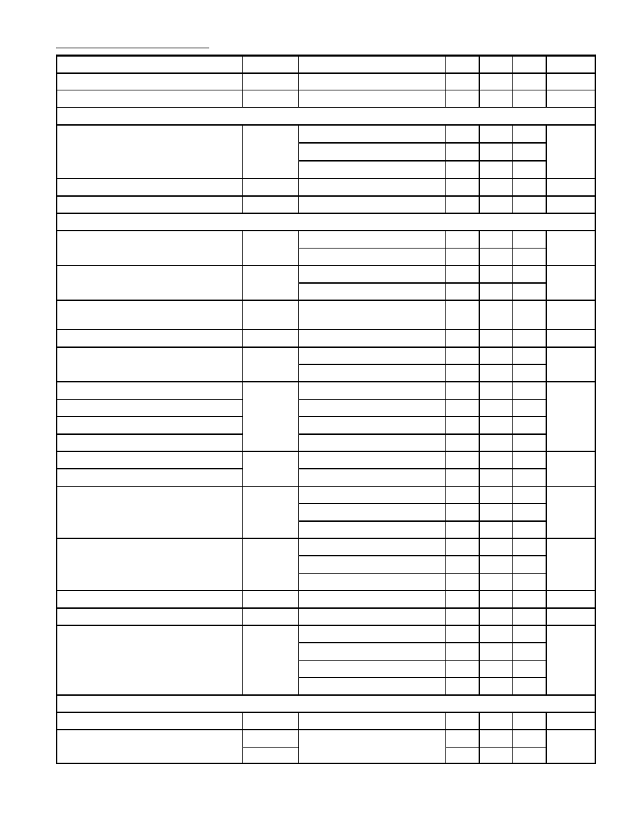
Electrical Characteristics (Cont'd): (T
A
= +25
∞
C unless otherwise specified)
Parameter
Symbol
Test Conditions
Min
Typ
Max
Unit
Protective Operation (Cont'd) (V
9
= 15V, T
A
= +25
∞
C)
External Trigger Input
V
5
Enable Voltage, V
reg
= 0V
≠
2.2
2.4
V
Disable Voltage, V
reg
= 0V
2.0
2.2
≠
Supply Voltage Disabling
V
8
amd V
1
V1
9
6.7
7.4
7.8
V
V
Pin5
Zener Voltage
V
5
Pin5 Open
6.5
7.3
7.8
V
I
Pin5
I
5
V
Pin5
= 3.0V
≠
1.4
≠
µ
A
V
Pin5
= 0V
≠
≠11
≠
Turn≠On Time (Secondary Voltages)
t
on
≠
350
450
ms
Voltage Change
V
2
S
3
= Closed,
P
3
= 19W
≠
100
500
mV
S
2
= Closed,
P
2
= 15W
≠
500
1000
Stand≠By Operation
(Minimum Secondary Power: 3W)
V
2
S
1
= Open
≠
20
30
V
Switching Frequency During
Stand≠By Mode
f
70
75
≠
kHz
Primary Power Consumption
During Stand≠By Mode
P
prim
The Heat Sink Must Be Opti-
mized, Taking the Maximum
Data (T
J
, R
JC
, T
A
) into
Consideration
≠
10
15
VA
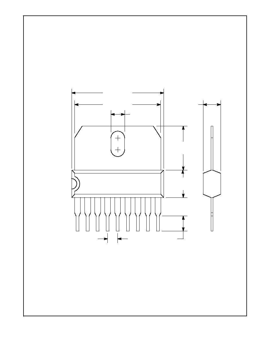
Pin Connection Diagram
V
CC
Zero Detection
Sawtooth Generator
Reference
Feedback
GND
Sink Output
Source Output
9
8
7
6
5
Shut Down
4
3
2
1
(Front View)