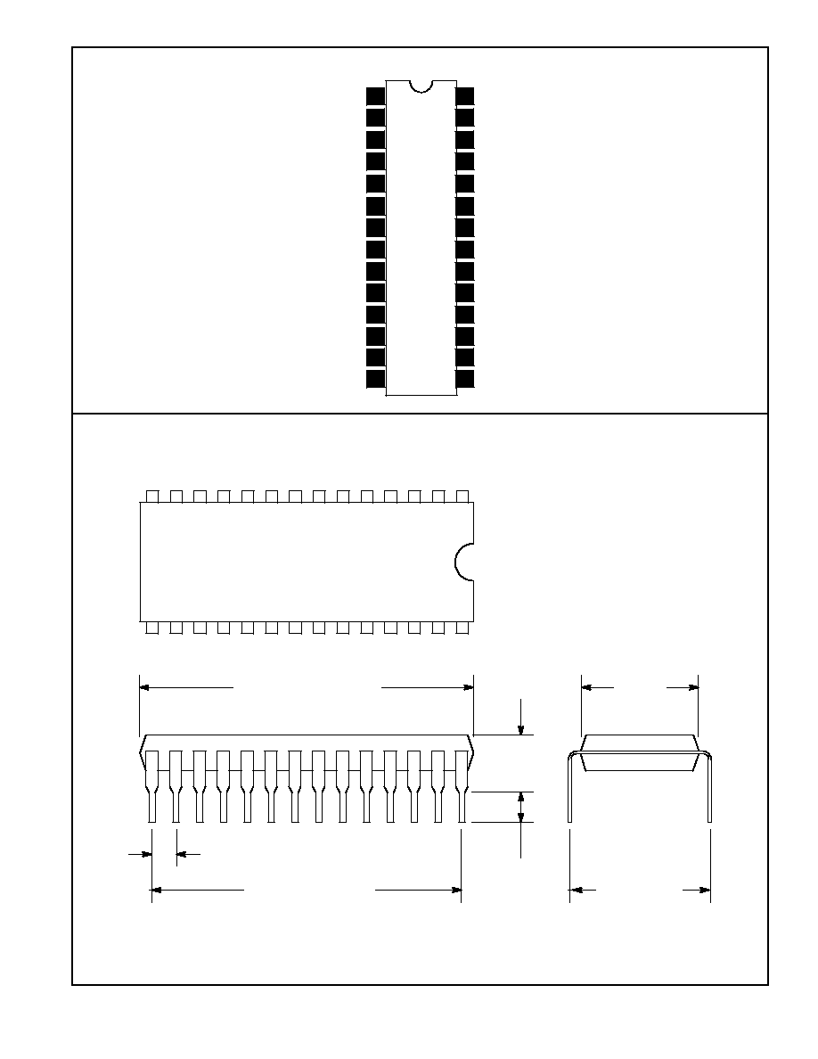
NTE1747
Integrated Circuit
TV Video Processing Circuit
Description:
The NTE1747 is an integrated circuit in a 28≠Lead DIP type package designed for color TV video and
chrominance signal processing circuit.
Features:
D
Including Video and Chrominance Signal Processing Circuit on a Single Chip, for Compact Set
Design
D
Including Circuit For Compensating Skin Color
Absolute Maximum Ratings: (T
A
= +25
∞
C unless otherwise specified)
Supply Voltage, V
CC
+14.4V
. . . . . . . . . . . . . . . . . . . . . . . . . . . . . . . . . . . . . . . . . . . . . . . . . . . . . . . . . . . . .
Circuit Voltage, V
2,3,10,11≠12,19,20,28≠9
0V to +14.4V
. . . . . . . . . . . . . . . . . . . . . . . . . . . . . . . . . . . . . . . . .
Circuit Current, I
25,26,27,28,29
≠40mA to 0mA
. . . . . . . . . . . . . . . . . . . . . . . . . . . . . . . . . . . . . . . . . . . . . . .
Power Dissipation, P
D
1200mW
. . . . . . . . . . . . . . . . . . . . . . . . . . . . . . . . . . . . . . . . . . . . . . . . . . . . . . . . .
Operating Ambient Temperature Range, T
opr
≠20
∞
to +70
∞
C
. . . . . . . . . . . . . . . . . . . . . . . . . . . . . . . . . .
Storage Temperature Range, T
stg
≠55
∞
to +150
∞
C
. . . . . . . . . . . . . . . . . . . . . . . . . . . . . . . . . . . . . . . . . .
Electrical Characteristics: (T
A
= +25
∞
C unless otherwise specified)
Parameter
Symbol
Test Conditions
Min
Typ
Max
Unit
Total Circuit Current
I
tot
V
CC
= 12V
40
54
67
mA
Demodulation Color Difference
Output Voltage
e
o(max)
Rainbow 150mV
P≠P
, Contrast Max.,
Color Max.
4.6
5.3
6.0
V
p≠p
Demodulation Color Difference
Output Voltage
e
o(typ)
Rainbow 150mV
P≠P
, Contrast Max.,
Color Typ.
1.35
1.75
2.15
V
p≠p
ACC Characteristics
ACC
Rainbow 15mV
P≠P
, ACC≠eo Typ
0.65
0.88
1.05
times
Oscillation Frequency
f
osc
Difference between Pin8 input invalid
signal & standard sample
≠
≠
±
150
H
z
f
osc
Change with Supply Voltage
D
f
osc
/V
CC
V
CC
= 12V
±
20%, for V
CC
= 12V
≠
≠
120
Hz
f
osc
Change with Ambient
Temperature
D
f
osc
/T
A
T
A
= ≠20
∞
to +70
∞
C, for T
A
= +25
∞
C
0
1.5
2.5
Hz/deg.
Control Sensitivity
b
Change to Pin18
D
f when V
1
(8.6V) and
V
2
(8.2V) are applied to Pin15.
1.9
2.5
3.2
Hz.mV
Electrical Characteristics (Cont'd): (T
A
= +25
∞
C unless otherwise specified)
Parameter
Symbol
Test Conditions
Min
Typ
Max
Unit
Phase Detector
µ
Apply
D
0≠changed frequency for burst
phase to Pin18.
27
46
64
mV/deg
Phase Hold Characteristics
Df
Df
=
1 (
m
.
b
) x 100
≠
1.0
1.6
deg/
100Hz
APC Pull≠in Range
f
APC
Rainbow 150mV
P≠P
measured by
changing burst frequency
±
550
±
800
≠
Hz
Demodulation Output Ratio
R/B
Demodulator input 0.5V
P≠P
,
f = 3.59MHz
0.84
0.93
1.02
times
Demodulation Output Ratio
G/B
Demodulator input 0.5V
P≠P
,
f = 3.59MHz
0.25
0.29
0.33
times
Demodulation Angle
<
R
Demodulator input 0.5V
P≠P
,
f = 3.59MHz, LB = 0dg
86.5
90.0
94.5
deg.
Demodulation Angle
<
G
Demodulator input 0.5V
P≠P
,
f = 3.59MHz, LB = 0dg
229
236
243
deg.
Color Killer Level
e
k
Attenuation from rainbow 150mV
P≠P
(=0dB) to killer operation
≠35
≠40
≠45
dB
Video Voltage Amplification
A
V1
Sine wave input 0.3V
P≠P
at 20kHz,
contrast max., picture min.
7.0
7.7
8.4
times
A
V2
Sine wave input 0.3V
P≠P
at 20kHz,
contrast 75%
6.3
7.0
7.6
times
DC Transfer Rate
T
DC
Video input 0.5V
P≠P
(stair step),
APL10 % to 90%. Contrast max.
Picture min.
86.0
90.5
95.0
%
Differential Gain
DG
Video input 0.5V
p≠p
(stair step),
APL10
90%. Contrast max.
picture min.
≠
≠
5
%
Demodulation DC Output Voltage
E
O(DC)
Input invalid signal, V
CO
oscillation,
demodulator outputs
7.20
7.60
8.05
V
DC Voltage Difference Between
Demodulation Outputs
D
E
X≠Y
Differential voltage of demodulator
outputs
≠
≠
300
mV
D
E
O
Change with Supply Volt-
age
D
E
X≠Y
/V
C
C
V
CC
= 12V
±
20%, for V
CC
= 12V
≠
0
±
60
mV
D
E
O
Change with Ambient
Temperature
D
E
X≠Y
/T
A
T
A
= ≠20
+70
∞
C. for T
A
= +25
∞
C
≠
0
±
60
mV
AIC Switching Level
V
SW
f = 3.58MHz, Pin21 level when
Pin 0 = 10V
160
260
340
mV
p≠p
Chroma Voltage Gain
G
Vchroma
Chroma/Burst 350/150mV
P≠P
,
Phase 123
1.6
2.2
2.7
V
p≠p
AIC Voltage Gain
G
vAIC
Chroma/Burst 200/150mV
P≠P
,
Phase 123' color killer OFF
14.5
19.0
23.5
dB
AIC Sensitivity
S
AIC
Chroma/Burst 300/100mV
P≠P
,
Phase 0 tint center
0.7
1.15
1.5
V
p≠p
Phase Compensation Center
Q
0
115
123
134
deg.
Phase Compensation Range
Q
c1
100
112
124
deg.
Phase Compensation Range
Q
c2
Chroma/Burst 150mV
P≠P
≠108
≠120
≠132
deg.
Phase Compensations Quantity
Q
Q1
Color Compensation ON
17
21.5
26
deg.
Phase Compensations Quantity
Q
Q2
≠18
≠22.5
≠28
deg.
Max. Phase Compensation
Q
Qmax1
51
59
67
deg.
Quantity
Q
Qmax2
≠55
≠63
≠71
deg.