
NTE1765
Integrated Circuit
Dual Channel Current Mode Controller
Description:
The NTE1765 is a high performance, fixed frequency, dual current mode controller in a 16ÙLead DIP
type package. This device is specifically designed for OffÙLine and DC to DC converter applications
offering the designer a cost effective solution with minimal external components. The NTE1765 fea-
tures a unique oscillator for precise duty cycle limit and frequency control, a temperature compen-
sated reference, two high gain error amplifiers, two current sensing comparators, drive output 2 en-
able pin, and two high current totem pole outputs ideally suited for driving power MOSFETS.
Also included are protective features consisting of input and reference undervoltage lockouts each
with hysteresis, cycleÙbyÙcycle current limiting, and a latch for single pulse metering of each output.
Features:
D
Unique Oscillator for Precise Duty Cycle Limit and Frequency Control
D
Current Mode Operation to 500kHz
D
Automatic Feed Forward Compensation
D
Separate Latching PWMs for CycleÙByÙCycle Current Limiting
D
Internally Trimmed Reference with Undervoltage Lockout
D
Drive Output 2 Enable Pin
D
Two High Current Totem Pole Outputs
D
Input Undervoltage Lockout with Hysteresis
D
Low StartÙUp and Operating Current
Absolute Maximum Ratings:
Total Power Supply Current, I
CC
50mA
. . . . . . . . . . . . . . . . . . . . . . . . . . . . . . . . . . . . . . . . . . . . . . . . . . . .
Zener Current, I
Z
50mA
. . . . . . . . . . . . . . . . . . . . . . . . . . . . . . . . . . . . . . . . . . . . . . . . . . . . . . . . . . . . . . . . .
Output Current, Source or Sink (Note 1), I
O
1A
. . . . . . . . . . . . . . . . . . . . . . . . . . . . . . . . . . . . . . . . . . . . .
Output Energy (Capacitive Load per Cycle), W
5.0
ç
J
. . . . . . . . . . . . . . . . . . . . . . . . . . . . . . . . . . . . . . .
Current Sense, Enable and Voltage Feedback Inputs, V
in
Ù0.3 to +5.5V
. . . . . . . . . . . . . . . . . . . . . . .
Sync Input, High State (Voltage), V
IH
5.5V
. . . . . . . . . . . . . . . . . . . . . . . . . . . . . . . . . . . . . . . . . . . . . . . .
Sync Input, Low State (Reverse Current), I
IL
Ù5.0mA
. . . . . . . . . . . . . . . . . . . . . . . . . . . . . . . . . . . . . . .
Error Amp Output Sink Current, I
O
10mA
. . . . . . . . . . . . . . . . . . . . . . . . . . . . . . . . . . . . . . . . . . . . . . . . . .
Maximum Power Dissipation (T
A
= +25
¯
C), P
D
1.25mW
. . . . . . . . . . . . . . . . . . . . . . . . . . . . . . . . . . . . .
Thermal Resistance, JunctionÙtoÙAmbient, R
thJA
100
¯
C/W
. . . . . . . . . . . . . . . . . . . . . . . . . . . . . . . . . .
Operating Junction Temperature, T
J
+150
¯
C
. . . . . . . . . . . . . . . . . . . . . . . . . . . . . . . . . . . . . . . . . . . . . . .
Operating Ambient Temperature Range, T
A
0
¯
to +70
¯
C
. . . . . . . . . . . . . . . . . . . . . . . . . . . . . . . . . . . . .
Storage Temperature Range, T
stg
Ù65
¯
to +150
¯
C
. . . . . . . . . . . . . . . . . . . . . . . . . . . . . . . . . . . . . . . . . .
Note 1. Maximum package power dissipation limits must be observed.

V Compensation
V Current Sense
Electrical Characteristics: (V
CC
= 15V (Note 2), R
T
= 8.2k
, C
T
= 3.3nF, Note 3 unless otherwise
specified)
Parameter
Symbol
Test Conditions
Min
Typ
Max
Unit
Reference Section
Reference Output Voltage
V
ref
I
O
= 1mA, T
J
= +25
¯
C
4.9
5.0
5.1
V
Line Regulation
Reg
line
V
CC
= 11V to 15V
Ù
2.0
20
mV
Load Regulation
Reg
load
I
O
= 1mA to 10mA
Ù
3.0
25
mV
Total Output Variation over Line,
Load and Temperature
V
ref
4.85
Ù
5.15
V
Output Short Circuit Current
I
SC
30
100
Ù
mA
Oscillator and PWM Sections
Total Frequency Variation over Line
and Temperature
f
OSC
V
CC
= 11V to 15V, T
A
= 0
¯
to +70
¯
C
46.5
49.0
51.5
kHz
Frequency Change with Voltage
f
OSC
/
V
V
CC
= 11V to 15V
Ù
0.2
1.0
%
Duty Cycle at each Output
Maximum
DC
max
46.0
49.5
52.0
%
Minimum
DC
min
Ù
Ù
0
%
Sync Input Current
High State
I
IH
V
in
= 2.4V
Ù
170
250
ç
A
Low State
I
IL
V
in
= 0.8V
Ù
80
160
ç
A
Error Amplifiers
Voltage Feedback Input
V
FB
V
O
= 2.5V
2.42
2.50
2.58
V
Input Bias Current
I
IB
V
FB
= 5V
Ù
Ù0.1
Ù1.0
ç
A
OpenÙLoop Voltage Gain
A
VOL
V
O
= 2V to 4V
65
100
Ù
dB
Unity Gain Bandwidth
BW
T
J
= +25
¯
C
0.7
1.0
Ù
MHz
Power Supply Rejection Ratio
PSRR
V
CC
= 11V to 15V
60
90
Ù
dB
Output Current
Source
I
Source
V
O
= 3V, V
FB
= 2.3V
Ù0.45
2.0
Ù
Ù1.0
Ù
Ù
mA
mA
Sink
I
Sink
V
O
= 1.2V, V
FB
= 2.7V
Ù
12
Ù
mA
Output Voltage Swing
High State
V
OH
R
L
= 15k to GND, V
FB
= 2.3V
5.0
6.2
Ù
V
Low State
V
OL
R
L
= 15k to V
ref
, V
FB
= 2.7V
Ù
0.8
1.1
V
Current Sense Section
Current Sense Input Voltage Gain
A
V
Note 4, Note 5
2.75
3.00
3.25
V/V
Max. Current Sense Input Threshold
V
th
Note 4
430
480
530
mV
Input Bias Current
I
IB
Ù
Ù2
Ù10
ç
A
Propagation Delay (Current Sense
Input to Output
t
PLN(IN/OUT)
Ù
150
300
ns
Note 2. Adjust V
CC
above the StartÙUp threshold before setting to 15V.
Note 3. For typical values, T
A
= +25C; for Min/Max values, T
A
= 0
¯
to +70
¯
C. Low duty cycle pulse
techniques are used during test to maintain junction temperature as close to ambient as pos-
sible.
Note 4. This parameter is measured at the latch trip point with V
fb
= 0V.
Note 5. Comparator gain is defined as A
V
=
Electrical Characteristics (Cont'd):
(V
CC
= 15V (Note 2), R
T
= 8.2k
, C
T
= 3.3nF, Note 3 unless
otherwise specified)
Parameter
Symbol
Test Conditions
Min
Typ
Max
Unit
Drive Output 2 Enable Pin
Enable Pin Voltage
High State
V
IH
Output 2 Enabled
3.5
Ù
V
ref
V
Low State
V
IL
Output 2 Disabled
0
Ù
1.5
V
Low State Input Current
I
IB
V
IL
= 0V
100
250
400
ç
A
Drive Outputs
Output Voltage
Low State
V
OL
I
Sink
= 20mA
Ù
0.1
0.4
V
I
Sink
= 200mA
Ù
1.6
2.5
V
High State
V
OH
I
Source
= 20mA
13.0
13.5
Ù
V
I
Source
= 200mA
12.0
13.4
Ù
V
Output Voltage with UVLO Activated
V
OL(UVLO)
V
CC
= 6V, I
Sink
= 1mA
Ù
0.1
1.1
V
Output Voltage Rise Time
t
r
C
L
= 1nF
Ù
28
150
ns
Output Voltage Fall Time
t
f
C
L
= 1nF
Ù
25
150
ns
Undervoltage Lockout Section
StartÙUp Threshold
V
th
13
14
15
V
Min. Operating Voltage After TurnÙOn
V
CC(min)
9.0
10.0
11.0
V
Total Device
Power Supply Current
StartÙUp
I
CC
V
CC
= 12V
Ù
0.6
1.0
mA
Operating
Note 2
Ù
20
25
mA
Power Supply Zener Voltage
V
Z
I
CC
= 30mA
15.5
17.0
19.0
V
Note 2. Adjust V
CC
above the StartÙUp threshold before setting to 15V.
Note 3. For typical values, T
A
= +25C; for Min/Max values, T
A
= 0
¯
to +70
¯
C. Low duty cycle pulse
techniques are used during test to maintain junction temperature as close to ambient as pos-
sible.
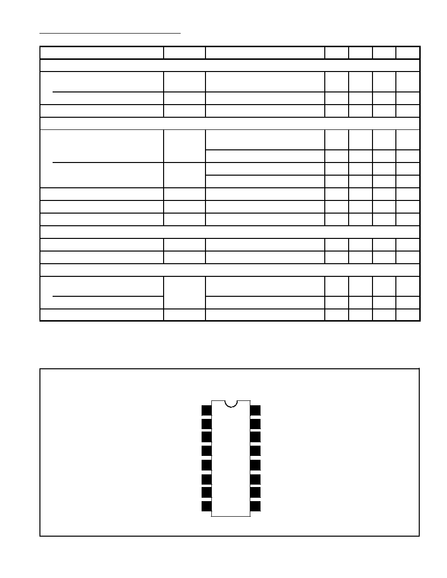
Pin Connection Diagram
V
ref
V
CC
R
T
C
T
Compensation 1
GND
Drive Output 1
Current Sense 1
Voltage Feedback 1
Voltage Feedback 2
Drive GND
Current Sense 2
Drive Output 2
Compensation 2
Drive Output 2 Enable
Sync Input
1
2
3
4
5
6
7
8
16
15
14
13
12
11
10
9
