 | –≠–ª–µ–∫—Ç—Ä–æ–Ω–Ω—ã–π –∫–æ–º–ø–æ–Ω–µ–Ω—Ç: NTE1790 | –°–∫–∞—á–∞—Ç—å:  PDF PDF  ZIP ZIP |
NTE1790
Integrated Circuit
Video IF, Chroma Deflection
Description:
The NTE1790 combines all the functions required for an NTSC color TV system on a 64≠Lead DIP
shrink type plastic package. This device is designed to have wide application capability, from a funda-
mental CTV application to a high≠end MPX CTV with quasi≠parallel SIF system, with minimal external
parts and adjustments. A quasi≠parallel SIF system assures buzz free sound reproduction.
Features:
PIF Section
D
3≠Stage Variable Gain PIF Amplifier
D
High Speed Peak AGC with Dual Time Constants
D
Single End AFT Output with Defeat Function
D
A Delayed RF AGC Output (Reverse AGC)
D
Sync Positive Detected Video Output Polarity
D
Internal Black/White Noise Inverter
Quasi≠Parallel Inter Carrier Detector
D
3≠Stage Variable Gain Intercarrier IF Amplifier
D
Independent Peak AGC
D
Intercarrier Detector with 90 deg. Carrier Shifter
SIF Section:
D
3≠Stage Limiter Amplifier
D
Differential Peak Detector
D
Separated Detector Output and Electronic Attenuater Input for Multiplex TV Sound Reception
D
Excellent Electronic Attenuater
D
Preamplifier with an NF Terminal
Video Section:
D
2nd Order Picture Sharpness (DC Control)
D
Contrast Control with Uni≠Color Function
D
Brightness Control with Pedestal Clamping Circuit (Adjustable DC Restoration Ratio)
D
Internal Vertical Blanking
Chroma Section:
D
ACC Circuit
D
Color Control Circuit
D
Uni≠Color Control Circuit
D
Adjustment Free APC Circuit
D
Tint Control Circuit With Sync Pulse Output
D
Color Differential Outputs

Deflection Section:
D
Excellent Sync Separator
D
Adjustment Free Count Down System
D
Stable Vertical Synchronization
D
Saw≠Tooth Type AFC
D
Horizontal Pre≠Driver
D
X≠Ray Protector
D
Vertical Drive Amplifier
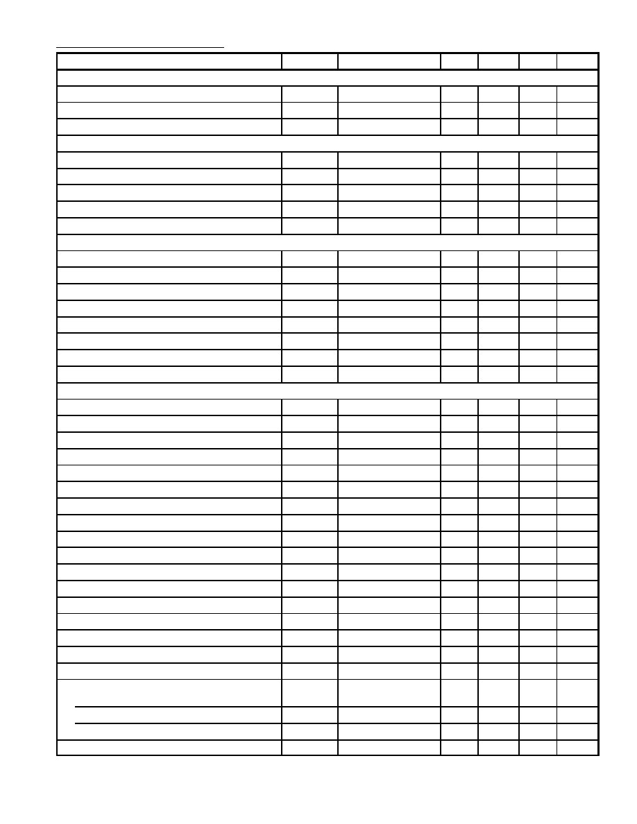
Absolute Maximum Ratings: (T
A
= +25
∞
C unless otherwise specified)
Supply Voltage, V
CC
12V
. . . . . . . . . . . . . . . . . . . . . . . . . . . . . . . . . . . . . . . . . . . . . . . . . . . . . . . . . . . . . . . .
Input Signal Level, e
in
5V
p≠p
. . . . . . . . . . . . . . . . . . . . . . . . . . . . . . . . . . . . . . . . . . . . . . . . . . . . . . . . . . . . .
RF AGC Voltage, V
RF
AGC
15V
. . . . . . . . . . . . . . . . . . . . . . . . . . . . . . . . . . . . . . . . . . . . . . . . . . . . . . . . . .
Horizontal Section Supply Voltage, V
CC
H
12V
. . . . . . . . . . . . . . . . . . . . . . . . . . . . . . . . . . . . . . . . . . . . . .
Power Dissipation, P
D
2660mW
. . . . . . . . . . . . . . . . . . . . . . . . . . . . . . . . . . . . . . . . . . . . . . . . . . . . . . . . .
Derate Above 25
∞
C
212mW/
∞
C
. . . . . . . . . . . . . . . . . . . . . . . . . . . . . . . . . . . . . . . . . . . . . . . . . . . . .
Operating Temperature Range, T
opr
≠20
∞
to +65
∞
C
. . . . . . . . . . . . . . . . . . . . . . . . . . . . . . . . . . . . . . . . .
Storage Temperature Range, T
stg
≠55
∞
to +150
∞
C
. . . . . . . . . . . . . . . . . . . . . . . . . . . . . . . . . . . . . . . . . .
Recommended Supply Voltage:
Parameter
Symbol
Test Conditions
Min
Typ
Max
Unit
PIF Section (Pin19)
8.5
9.0
9.5
V
QIF, SIF Section (Pin37)
8.5
9.0
9.5
V
Video, Chroma, Deflection Section (Pin16)
8.5
9.0
9.5
V
Horizontal Section (Pin58)
6.3
6.8
7.3
V
AC Characteristics: (T
A
= +25
∞
C, V
CC
= 9V, 6.8V unless otherwise specified)
Parameter
Symbol
Test Conditions
Min
Typ
Max
Unit
PIF Section
Input Sensitivity
v
in
70
120
200
µ
V
rms
IF AGC Gain Reduction
GR
60
64
≠
dB
Video Bandwidth
BW
4.5
≠
≠
MHz
Video Ripple
≠
0
±
1
dB
Differential Phase
DP
≠
≠
5
deg.
Differential Gain
DG
≠
≠
10
%
Video White Peak
V
47
3.2
3.7
4.4
V
Noise Inverter
White Inverter
V
W
TH
2.7
3.0
3.3
V
White Clamp
V
W
CL
4.6
5.0
5.4
V
Black Inverter
V
B
TH
6.4
6.8
7.2
V
Black Clamp
V
B
CL
4.8
5.2
5.6
V
Carrier Suppression
40
≠
≠
dB
Harmonics Suppression
I
2nd
40
≠
≠
dB
Input Impedance
R
i
PIF
1.75
2.5
3.25
k
Input Capacitance
C
i
PIF
2
4
8
pF
AFT Center Voltage
No Signal
5.1
6.5
10.3
V
Offset
≠
≠
±
3
V
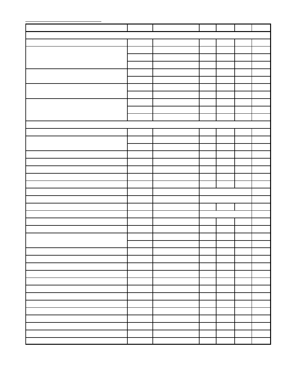
AC Characteristics (Cont'd): (T
A
= +25
∞
C, V
CC
= 9V, 6.8V unless otherwise specified)
Parameter
Symbol
Test Conditions
Min
Typ
Max
Unit
PIF Section (Cont'd)
AFT Sensitivity
≠
15
25
kHz/V
AFT Voltge Swing
A
6
11
≠
V
920kHz Beat
I
920
32
≠
≠
dB
QIF Section
Input Sensitivity
v
in
Q
70
120
200
µ
V
rms
4.5MHz Output Level
1.0
1.5
2.0
V
P≠P
AGC Gain Reduction
GR Q
60
64
≠
dB
Input Impedance
R
i
QIF
1.75
2.5
3.25
k
Input Capacitance
C
i
QIF
2
4
10
pF
SIF Section
Limiting Sensitivity
v
LIM
115
140
180
µ
V
rms
Detected Output
v
OD
130
155
≠
mV
rms
AM Rejection
AMR
20
≠
≠
dB
SIF Bandwidth
BW SIF
120
160
≠
kHz
THD Bandwidth
BD THD
THD = 1.5%
100
140
≠
kHz
Attenuation AC Gain
G
V
ATT
4
6
8
dB
Maximum Attenuation
ATT
max
70
≠
≠
dB
AF Amp AC Gain
G
V
AF
≠
18
≠
dB
Video Section
Input Impedance, Pin52
z
i52
1.8
2.5
3.2
k
Input Impedance, Pin53
z
i53
14
19
24
k
Video Output Impedance
z
o13
15
30
100
Brightness Control Voltage
V
BR
3.9
4.3
4.7
V
Brightness Sensitivity
G
BR
3.0
3.4
3.8
Minimum Linear Video Input
V
di1
≠
2.3
2.7
V
Maximum Linear Video Input
V
di2
5.0
5.5
≠
V
Video Input Dynamic Range
V
di
2.7
3.2
≠
V
P≠P
Minimum Video Output
V
do1
0
0.3
1.1
V
Maximum Video Output
V
do2
7.5
7.9
9.0
V
2nd Order Differential Input Dynamic Range
V
diP
0.3
0.4
0.5
V
P≠P
Video Gain
G
V
3.2
4.2
4.9
Frequency Response
G
f
≠3.2
≠1.0
≠0.8
dB
Contrast Control Voltage Range
dVct
0.71
1.4
2.09
V
Contrast Control Range
dGct
11
12
13
dB
Contrast Control Center Voltage
V
cto
4.2
4.5
4.8
V
Frequency Response Dependence
dG
f
≠
0
0.9
dB
Frequency Response at
Minimum Picture Control
dG
ps
min
≠10
≠6
≠3.4
dB
Maximum Control
dG
ps
max
10
11
12
dB
Center Control
dG
ps
0
≠3.0
≠1.7
0
dB
Picture Control Voltage Range
dV
ps
0.68
1.2
1.43
V

AC Characteristics (Cont'd): (T
A
= +25
∞
C, V
CC
= 9V, 6.8V unless otherwise specified)
Parameter
Symbol
Test Conditions
Min
Typ
Max
Unit
Video Section (Cont'd)
Vertical Blanking Pulse Output Level
V
V
8.0
8.9
9.0
V
Horizontal Blanking Pulse Detection Level
V
H
8.0
8.4
8.8
V
Horizontal Blanking Input Current
I
H
1.5
2.5
4.0
mA
Chroma Section
ACC Characteristics
e
a
0.72
1.54
≠
V
P≠P
A
≠
1.0
1.3
V
P≠P
Demodulator Color Differential Output
e
R1
1.0
1.47
2.0
V
P≠P
e
G1
0.35
0.51
0.71
V
P≠P
e
B1
1.19
1.75
2.44
V
P≠P
Color Killer Residual
e
KR
≠
≠
10
mV
e
KG
≠
≠
10
mV
e
KB
≠
≠
10
mV
Color Control Residual
e
CR
≠
≠
10
mV
e
CG
≠
≠
10
mV
e
CB
≠
≠
10
mV
Color Control Voltage
V
3
4.1
4.6
5.1
V
Color Control Range
dV
3
0.7
1.4
2.1
V
Uni≠Color Control Range
e
U
10.5
12.0
13.5
dB
Uni≠Color Control Voltage
V
8
4.1
4.6
5.1
V
Uni≠Color Control Range
dV
8
0.7
1.4
2.1
V
Color Control Phase Change
d0
C
≠
≠
5
deg.
Uni≠Color Control Phase Change
d0
U
≠
≠
7
deg.
Maximum Input of Bandpass Amplifier
e
M
0.48
0.6
≠
V
P≠P
Tint Control Range
d0
78
100
131
deg.
Tint Control Range
d0
1
35
55
≠
deg.
d0
2
31
45
≠
deg.
Tint Control Voltage
V
2
4.0
4.6
5.1
V
Tint Control Voltage Range
dV
2
0.25
0.5
0.75
V
Sync Pulse Width
S
t
≠
4.5
≠
µ
s
Sync Pulse, High
V
S1
≠
5.42
≠
V
Sync Pulse, Low
V
S2
≠
3.6
≠
V
APC Frequency Control Sensitivity
b
≠
7.0
≠
Hz/mV
APC Pull≠In Range
f
P
≠
1.3
≠
Hz
APC Hold Range
f
Hld
≠
2.5
≠
Hz
Sweeper Amplitude
SEV1
≠
4.0
≠
V
SEV2
≠
3.0
≠
V
SEV
0.8
1.0
1.2
V
P≠P
Sweeper Period
tE1
4
7
10
ms
tE2
35
55
77
ms
tE
39
62
87
ms
Killer Level
e
K
0.4
1.0
≠
mV
P≠P
AC Characteristics (Cont'd): (T
A
= +25
∞
C, V
CC
= 9V, 6.8V unless otherwise specified)
Parameter
Symbol
Test Conditions
Min
Typ
Max
Unit
Chroma Section (Cont'd)
Demod Output DC Voltage
R.G.B
4.9
5.6
6.4
V
Maximum Demod Output
E
R
3.9
4.6
5.9
V
P≠P
E
G
1.3
1.54
2.0
V
P≠P
E
B
3.9
4.6
5.9
V
P≠P
Demod Relative Amplitude
R/B
0.71
0.84
0.97
G/B
0.23
0.29
0.35
Demod Relative Phase
R≠B
102
109
116
deg.
G≠B
227
242
252
deg.
Demod Output Residual Carrier
ECR
≠
≠
300
mV
P≠P
ECG
≠
≠
300
mV
P≠P
ECB
≠
≠
300
mV
P≠P
Deflection Section
Pin57 Input Current
I
R57
≠
≠
1
µ
A
Sync Signal Delay Time
t
pdr
0
40
100
ns
t
pdf
0
60
100
ns
Pin56 Terminal Voltage
V
56
5.2
5.7
6.2
V
Pin56 Output Current
I
O56
2.0
3.0
4.9
µ
A
Gate Pulse Width
T
pw8
2.7
3.0
3.6
µ
s
Gate Pulse Delay
t
pd8
0.2
0.4
0.6
µ
s
Chroma Sweep Pulse Width
T
cwt
≠
8H
≠
Vertical Masking Pulse (Gate)
256.25H to 10.25H
Vertical Masking Pulse (Horizontal AFC)
256.25H to 10.25H
Vertical Sync Integrating Time Constants
T
VS
12
16
34
µ
s
Vertical Retrace Pulse Width
T
VO55
10H / 11H
Vertical Amp Gain
G
VA54
8.7
9.5
10.7
dB
Vertical Amp Input Dynamic Range
V
i55
1.1
1.6
≠
V
Vertical Amp Output Dynamic Range
V
H55
5.1
6.2
7.3
V
V
L55
1.1
1.9
3.1
V
Vertical Amp Maximum Output Current
I
O54
11.2
16.8
25.0
mA
Horizontal 32f
H
Oscillator Starting Voltage
V
CC58
1
1.7
2.0
2.5
V
Horizontal Drive Output Starting Voltage
V
CC58
2
2.7
3.0
3.2
V
Horizontal Drive Output Starting Current
I
CC58
4.0
5.4
6.8
mA
Horizontal Oscillator Frequency
f
H
15654
15734
15814
Hz
f
H
temperature Drift
df
HT
40
70
100
Hz
f
H
V
CC
Coefficient
df
HV
0
≠20
≠40
Hz
Horizontal Output Duty
T
O64
39
41
43
%
Horizontal Output Saturation Voltage
V
OL64
0
0.2
0.3
V
f
H
Pull≠In Range
df
pull
±
550
±
750
±
880
Hz
f
H
Hold Range
df
hold
±
550
±
750
±
880
Hz
X'Ray Sense Voltage
V
in1
1.1
1.3
1.5
V
X'Ray Sense Current
I
in1
0.05
0.4
1.0
µ
A

AC Characteristics (Cont'd): (T
A
= +25
∞
C, V
CC
= 9V, 6.8V unless otherwise specified)
Parameter
Symbol
Test Conditions
Min
Typ
Max
Unit
Deflection Section (Cont'd)
X'Ray Protector Recovering Voltage
V
Hold
1.0
1.4
1.7
V
Vertical Sync Pull≠In Range
f
PV1
≠
232.5H
≠
f
PV2
≠
296.5H
≠
32f
H
VCO
32f
H
VCO
32f
H
VCO
H V
CC
(6.8V)
9V V
CC
Q≠SIF
9V V
CC
PIF
9V V
CC
V/C/D
f
SC
VCO
f
SC
VCO
Pin Connection Diagram
Sync Sep Time Constant
QIF Input
QIF Input
Pedestal Clamp
B ≠ Y Output
APC Filter
Killer Filter
Flyback Pulse Input
GND
GND
Sync Sep Input
1
2
3
4
X≠Ray Protect
Tint Control
Color Control
5
6
7
8
Contrast Control
64
63
62
61
Horiz Driver Output
60
AFC Time Constant
59
58
57
9
R ≠ Y Output
56
Vertical NFB
Vertical Output
10
G ≠ Y Output
11
55
54
Video Input
12
53
Differential Input
13
≠Y Output
52
Picture Sharpness
14
51
15
Brightness
50
Video Output
I/C Detector
GND
PIF AGC Time Constant
RF AGC Output
Video Detector Tank
16
17
Bypass
18
RF AGC Delay
19
20
PIF Input
49
Chroma Input
48
ACC Filter
47
46
45
Video Detector Tank
21
PIF Input
44
AFT Tank/Defeat
AFT Output
22
PIF AGC Time Constant
23
43
42
4.5MHz Output
24
41
GND
25
40
I/C Detector
26
39
27
QIF AGC Time Constant
38
Audio Input
Volume Control
FM Detector Tank
NFB
Preamp Output
28
37
SIF Input
29
36
SIF Bias
30
35
Detector Output
31
34
32
FM Detector Tank
33
2.270 (57.65) Max
1
32
64
33
.708 (18.0)
Min
.750 (19.0)
.236
(6.0)
Max
.106 (2.7) Min
.070 (1.78)