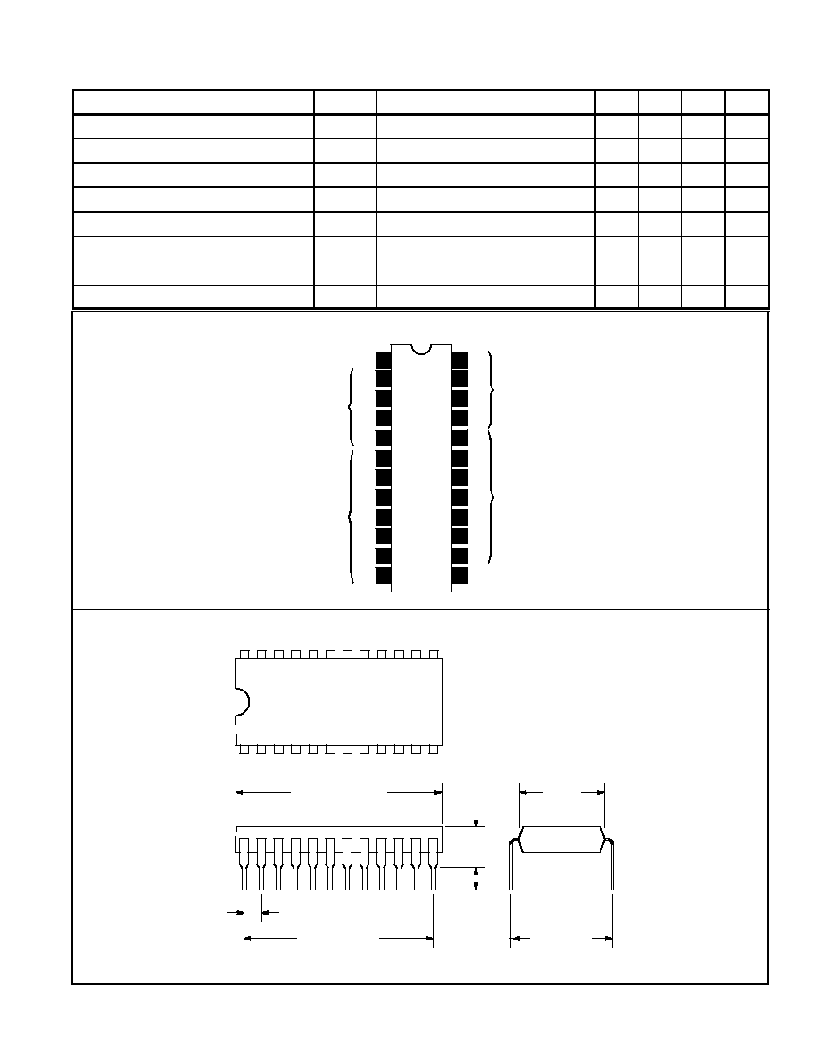
NTE2024
Integrated Circuit
2≠Digit BCD≠to≠7≠Segment Decoder/Driver
Features:
D
Separate BCD inputs and segment outputs for each digit
D
Input loading less than 15
µ
A
D
I
2
L logic with buffered inputs and outputs
D
Internal input overrange protection circuit
D
5V supply operation
D
Internal biasing circuits
D
Output drive capability of 25mA per segment
D
Open collector outputs drive indicators directly
Description:
The NTE2024 is a monolithic integrated circuit intended for 2≠digit display such as "numbers" for tV
and "CB" channel selection, and other 0≠99 numerical or counting for consumer or industrial indicator
applications. It consists of two independent BCD≠to≠7 segment decoder/drivers. Two sets of BCD
inputs are buffered with p≠n≠p differential amplifier stages internally referenced to 1.7V. Each of the
eight input terminals draws less than 15
µ
A and is provided with an internal protection circuit.
Decoding is accomplished with I
2
L ROM's. The fourteen output terminals are buffered with Darlington
pairs driving common≠emitter output transistors. Each output is capable of sinking 25mA for an LED
common≠anode display device. The supply≠voltage range (V
CC
) is intended to be 4.5V to 6V. The
output voltage (V
O
) must not exceed 12V, which provides for a wide range of common≠anode voltage
sources.
Absolute Maximum Ratings:
Supply Voltage, V
CC
6V
. . . . . . . . . . . . . . . . . . . . . . . . . . . . . . . . . . . . . . . . . . . . . . . . . . . . . . . . . . . . . . . .
Input≠Voltage (Min/Max)
≠0.3V
CC
V
. . . . . . . . . . . . . . . . . . . . . . . . . . . . . . . . . . . . . . . . . . . . . . . . . . . . . .
Input Current (Protection Circuit)
±
10mA
. . . . . . . . . . . . . . . . . . . . . . . . . . . . . . . . . . . . . . . . . . . . . . . . . .
Output Voltage, V
O
12V
. . . . . . . . . . . . . . . . . . . . . . . . . . . . . . . . . . . . . . . . . . . . . . . . . . . . . . . . . . . . . . . .
Output Segment Current, I
Display
25mA
. . . . . . . . . . . . . . . . . . . . . . . . . . . . . . . . . . . . . . . . . . . . . . . . . . .
Power Dissipation (T
A
+70
∞
C), P
D
400mW
. . . . . . . . . . . . . . . . . . . . . . . . . . . . . . . . . . . . . . . . . . . . . . .
Derate Linearly Above +70
∞
C 8.7mW/
∞
C
. . . . . . . . . . . . . . . . . . . . . . . . . . . . . . . . . . . . . . . . . . .
Operating Ambient temperature Range, T
opr
0
∞
to 70
∞
C
. . . . . . . . . . . . . . . . . . . . . . . . . . . . . . . . . . . .
StorageTemperature range, T
stg
≠55
∞
to +150
∞
C
. . . . . . . . . . . . . . . . . . . . . . . . . . . . . . . . . . . . . . . . . . . .
Lead Temperature (During Soldering, 1/16"
±
1/32" from case, 10sec max), T
L
+265
∞
C
. . . . . . . . . .