
NTE1802
Integrated Circuit
Power Amplifier for Car Stereo Radio,
12W/Ch or 24W BTL
Description:
The NTE1802 is an integrated classÙB output amplifier in a 13ÙLead SIP type package. This device
contains two identical amplifiers with different input stages which can be used for stereo or bridge ap-
plications. The gain of each amplifier is fixed at 20dB. A special feature of the NTE1802 is the mute/
standÙby switch.
Features:
D
Requires Few External Components
D
High Output Power (With Bootstrap)
D
Low Offset Voltage at Output
D
Fixed Gain
D
Good Ripple Rejection
D
Mute/StandÙBy Switch
D
Load Dump Protection
D
AC and DC ShortÙCircuit Safe
D
Thermally Protected
D
Reverse Polarity Safe
D
Capability to handle High Energy on Outputs
D
No SwitchÙOn/SwitchÙOff Pop
D
Flexible Leads
D
Low Thermal Resistance
D
Identical Inputs (Inverting and NonÙInverting)
Absolute Maximum Ratings:
Supply Voltage, V
P
Operating
18V
. . . . . . . . . . . . . . . . . . . . . . . . . . . . . . . . . . . . . . . . . . . . . . . . . . . . . . . . . . . . . . . . . . .
NonÙOperating
30V
. . . . . . . . . . . . . . . . . . . . . . . . . . . . . . . . . . . . . . . . . . . . . . . . . . . . . . . . . . . . . .
Load Dump Protected (During 50ms, t
r
> 2.5ms)
45V
. . . . . . . . . . . . . . . . . . . . . . . . . . . . . . . . .
AC and DC ShortÙCircuit Safe Voltage, V
PSC
18V
. . . . . . . . . . . . . . . . . . . . . . . . . . . . . . . . . . . . . . . . . .
Reverse Polarity, V
PR
6V
. . . . . . . . . . . . . . . . . . . . . . . . . . . . . . . . . . . . . . . . . . . . . . . . . . . . . . . . . . . . . . . .
Energy Handling Capability at Output (V
P
= 0V)
200mJ
. . . . . . . . . . . . . . . . . . . . . . . . . . . . . . . . . . . . .
NonÙRepetitive Peak Output Current, I
OSM
6A
. . . . . . . . . . . . . . . . . . . . . . . . . . . . . . . . . . . . . . . . . . . . .
Repetitive Peak Output Current, I
ORM
4A
. . . . . . . . . . . . . . . . . . . . . . . . . . . . . . . . . . . . . . . . . . . . . . . . . .
Total Power Dissipation, P
tot
25W
. . . . . . . . . . . . . . . . . . . . . . . . . . . . . . . . . . . . . . . . . . . . . . . . . . . . . . . .
Crystal Temperature, T
C
+150
¯
C
. . . . . . . . . . . . . . . . . . . . . . . . . . . . . . . . . . . . . . . . . . . . . . . . . . . . . . . . .
Storage Temperature Range, T
stg
Ù55
¯
to +150
¯
C
. . . . . . . . . . . . . . . . . . . . . . . . . . . . . . . . . . . . . . . . . .

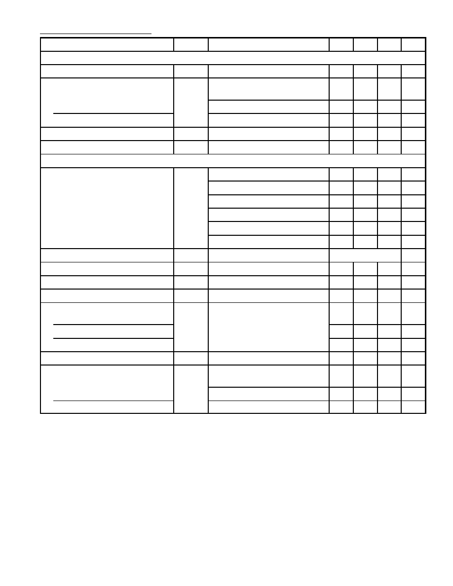
DC Characteristics: (V
P
= 14.4V, T
A
= +25
¯
C unless otherwise specified)
Parameter
Symbol
Test Conditions
Min
Typ
Max
Unit
Supply
Supply Voltage
V
P
Note 1
6.0
14.4
18.0
V
Quiescent Current
I
P
Ù
40
80
mA
DC Output Voltage
V
O
at approximately V
P
/2, Note 2
Ù
6.8
Ù
V
DC Output Offset Voltage
|
V
5Ù9
|
Ù
Ù
100
mV
Mute/StandÙby Switch
SwitchÙOn Voltage Level
V
ON
8.5
Ù
Ù
V
Mute Condition
V
mute
3.0
Ù
6.4
V
Output Signal in Mute Position
V
O
V
I
= 1V Max, f = 20Hz to 18kHz
Ù
*
2
mV
DC Output Offset Voltage
|
V
5Ù9
|
Ù
Ù
100
mV
StandÙBy Condition
V
sb
0
Ù
2
V
DC Current in StandÙBy Condition
I
sb
Ù
Ù
100
ç
A
SwithcÙOn Current
I
sw
Ù
12
40
ç
A
* Value to be fixed.
Note 1. The circuit is DC adjusted at V
P
= 6V to 18V and AC operating at V
P
n= 8.5V to 18V.
Note 2. At 18V < V
P
< 30V the DC output voltage
V
P
/2.
AC Characteristics: (V
P
= 14.4V, R
L
= 4
, f = 1kHz, T
A
= +25
¯
C unless otherwise specified)
Parameter
Symbol
Test Conditions
Min
Typ
Max
Unit
Stereo Applications
Output Power (Note 3)
P
O
THD = 0.5%
4.0
5.0
Ù
W
THD = 10%
5.5
6.0
Ù
W
THD = 10%, Note 4
6.0
7.0
Ù
W
R
L
= 2
, THD = 0.5%
7.5
8.5
Ù
W
R
L
= 2
, THD = 10%
10.0
11.0
Ù
W
R
L
= 2
, THD = 10%, Note 4
10.5
12.0
Ù
W
Low Frequency RollÙOff
f
L
Ù3dB, Note 5
Ù
45
Ù
Hz
High Frequency RollÙOff
f
H
Ù1dB
20
Ù
Ù
kHz
Closed Loop Voltage Gain
G
V
19
20
21
dB
Supply Voltage Ripple Rejection
ON
RR
Note 6
48
Ù
Ù
dB
Mute
48
Ù
Ù
dB
StandÙBy
80
Ù
Ù
dB
Note 3. Output power is measured directly at the output pins of the IC.
Note 4. With bootstrap and a 100k
resistor from Pin12 to the positive supply voltage (V
P
), value
of the bootstrap capacitor is 47
ç
F.
Note 5. Frequency response externally fixed.
Note 6. Ripple rejection measured at the output with a source impedance of 0
(maximum ripple
amplitude of 2V) and a frequency between 1kHz and 10kHz.
AC Characteristics (Cont'd): (V
P
= 14.4V, R
L
= 4
, f = 1kHz, T
A
= +25
¯
C unless otherwise specified)
Parameter
Symbol
Test Conditions
Min
Typ
Max
Unit
Stereo Applications (Cont'd)
Input Impedance
|Z
I
|
50
60
75
k
Noise Output Voltage
ON
V
no(rms)
R
S
= 0
, Note 7
Ù
50
Ù
ç
V
R
S
= 10k
, Note 7
Ù
70
100
ç
V
Mute
Note 8
Ù
60
Ù
ç
V
Channel Separation
R
S
= 10k
40
Ù
Ù
dB
Channel Balance
G
V
Ù
Ù
1
dB
BTL Application
Output Power
P
O
THD = 0.5%
15.5
17.0
Ù
W
THD = 10%
20.0
22.0
Ù
W
THD = 10%, Note 4
21.0
24.0
Ù
W
V
P
= 13.2V, THD = 0.5%
Ù
13.5
Ù
W
R
L
= 2
, THD = 10%
Ù
17.0
Ù
W
R
L
= 2
, THD = 10%, Note 4
Ù
19.0
Ù
W
Power Bandwidth
B
W
THD = 0.5%, P
O
= 15W
20 to 15000
Hz
Low Frequency RollÙOff
f
L
Ù3dB, Note 5
Ù
25
Ù
Hz
High Frequency RollÙOff
f
H
Ù1dB
20
Ù
Ù
kHz
Closed Loop Voltage Gain
G
V
25
26
27
dB
Supply Voltage Ripple Rejection
ON
RR
Note 6
48
Ù
Ù
dB
Mute
48
Ù
Ù
dB
StandÙBy
80
Ù
Ù
dB
Input Impedance
|Z
I
|
25
30
38
k
Noise Output Voltage
ON
V
no(rms)
R
S
= 0
, Note 7
Ù
70
Ù
ç
V
R
S
= 10k
, Note 7
Ù
100
200
ç
V
Mute
Note 8
Ù
60
Ù
ç
V
Note 4. With bootstrap and a 100k
resistor from Pin12 to the positive supply voltage (V
P
), value
of the bootstrap capacitor is 47
ç
F.
Note 7. Noise voltage measured in a bandwidth of 20Hz to 20kHz.
Note 8. Noise output voltage independent of R
S
(V
I
= 0V).
