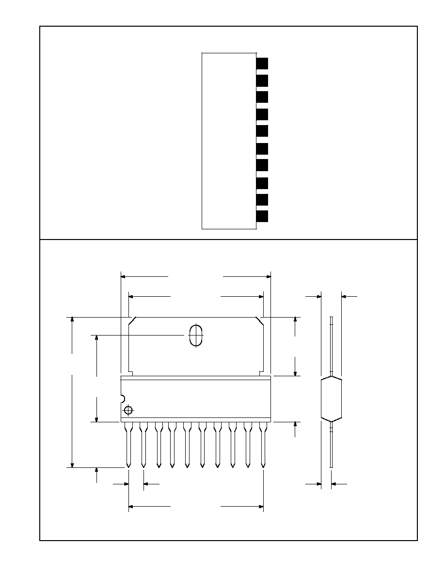
NTE1834
Integrated Circuit
Dual Reversible Motor Driver
Description:
The NTE1834 is a monolithic IC in a 10≠Lead SIP type package designed for use as a dual reversible
motor driver. This device contains two independent circuits designed for driving brush≠type DC mo-
tors. The control logic inputs are compatible with CMOS devices. The motor torque can be controlled
by varying the motor voltage with the control input (Pin8). With few external components required
and dual circuit configuration, the NTE1834 offers great benefits in terms of reduced components and
reduced circuit board space.
Features:
D
Dual Reversible Motor Drivers Implemented on a Single Chip (Simultaneous Dual Circuit Operation
is Not Possible)
D
Minimum External Components Required
D
Control Inputs Directly Compatible with CMOS Logic (Protection Resistors are Required if CMOS
Output Voltage Exceeds 5V)
D
Internal Motor Driving Power Transistors
D
Internal Surge Suppressors
D
Internal Thermal Shut≠Down Circuit
Applications:
D
VCRs
D
Tape Decks
Absolute Maximum Ratings: (T
A
= +25
∞
C unless otherwise specified)
Supply Voltage, V
CC
20V
. . . . . . . . . . . . . . . . . . . . . . . . . . . . . . . . . . . . . . . . . . . . . . . . . . . . . . . . . . . . . . . .
Input Voltage Range, V
i
≠0.3V to +5V
. . . . . . . . . . . . . . . . . . . . . . . . . . . . . . . . . . . . . . . . . . . . . . . . . . . . .
Output Current (Note 1), I
OUT
1.6A
. . . . . . . . . . . . . . . . . . . . . . . . . . . . . . . . . . . . . . . . . . . . . . . . . . . . . . .
Power Dissipation, P
D
2200mW
. . . . . . . . . . . . . . . . . . . . . . . . . . . . . . . . . . . . . . . . . . . . . . . . . . . . . . . . .
Operating Temperature Range, T
opr
≠25
∞
to +75
∞
C
. . . . . . . . . . . . . . . . . . . . . . . . . . . . . . . . . . . . . . . . .
Storage Temperature Range, T
stg
≠55
∞
to +125
∞
C
. . . . . . . . . . . . . . . . . . . . . . . . . . . . . . . . . . . . . . . . . .
Note 1. Pulse Width = 200
µ
s, Duty Cycle = 1%
Recommended Operating Conditions: (T
A
= +25
∞
C unless otherwise specified)
Parameter
Symbol
Test Conditions
Min
Typ
Max
Unit
Supply Voltage
V
CC
1
8
≠
18
V
V
CC
2
8
≠
18
V
V
R
0
≠
18
V

Electrical Characteristics: (T
A
= +25
∞
C, V
CC
= 12V unless otherwise specified)
Parameter
Symbol
Test Conditions
Min
Typ
Max
Unit
Supply Current
I
CC
R
L
=
, Pin4, Pin5, and Pin6 = "L" Level
≠
12
24
mA
Input Low Level Voltage
(Pin4, Pin5, and Pin6)
V
IL
≠
≠
1.0
V
Input High Level Voltage
(Pin4, Pin5, and Pin6)
V
IH
4.0
≠
≠
V
Output Low Level Voltage
(Pin4, Pin5, and Pin10)
V
OL
Pin8 = Open, I
O
= 500mA
≠
0.8
1.5
V
Output High Level Voltage
(Pin4, Pin5, and Pin10)
V
OH
Pin8 = Open, I
O
= 500mA
10
10.5
≠
V
Output Leakage Current
I
OL
R
L
=
, Pin4, Pin5, and Pin6 = "L" Level,
Current flowing to Pin9
≠
≠
1
mA
Voltage Stability
(Pin2)
V
2
V
R
= 6V with respect
I
O(2)
= 500mA
≠0.5
≠
0.5
V
(Pin3)
V
3
to Pin8
I
O(3)
= 500mA
≠0.5
≠
0.5
V
(Pin10)
V
10
I
O(10)
= 500mA
≠0.5
≠
0.5
V
Drain Current
(Pin2)
I
8 (2)
V
R
= 6V, I
O(2)
= 500mA, Pin2 = "H" Level
≠0.5
≠
0.5
V
(Pin3)
I
8 (3)
V
R
= 6V, I
O(3)
= 500mA, Pin3 = "H" Level
≠0.5
≠
0.5
V
(Pin10)
I
8 (10)
V
R
= 6V, I
O(10)
= 500mA, Pin10 = "H" Level
≠0.5
≠
0.5
V
Backlash Current
I
B
Sink current at Pin9 when Pin4, Pin5, and Pin6
are low and one output pin is at ≠1V
≠
≠
0.3
A
Thermal Shut≠Down Operate
Temperature
T
ON
≠
150
≠
∞
C
Thermal Shut≠Down Release
Temperature
T
OFF
≠
100
≠
∞
C
Input/Output Truth Table:
Input
Output
Function
Pin4
Pin5
Pin6
Pin10
Pin2
Pin3
L
L
X
L
L
L
Brake
H
L
L
H
L
OPEN
Current flows from Pin10 to Pin2
H
L
H
L
H
OPEN
Current flows from Pin2 to Pin10
L
H
L
H
OPEN
L
Current flows from Pin10 to Pin3
L
H
H
L
OPEN
H
Current flows from Pin3 to Pin10
H
H
X
L
L
L
Brake
X = Don't Care
Precautions:
1. While the control input pins of the NTE1834 can be directly connected to MOS logic outputs, it is
recommended that you insert a series protection resistor in the range 1k
to 10k
between the
devices.
2. To improve reliability, be sure to temporarily put the device in brake mode before reversing the
direction of rotation of the motor. A brake mode duration of more than 10
µ
s is recommended.
3. The recommended power on sequence is one in which V
CC
1 (Pin7) is the first turned on and the
last turned off.