NTE1898 & NTE1899
Integrated Circuit
Dual Audio Power Amp, 5.8W (22W BTL)
Description:
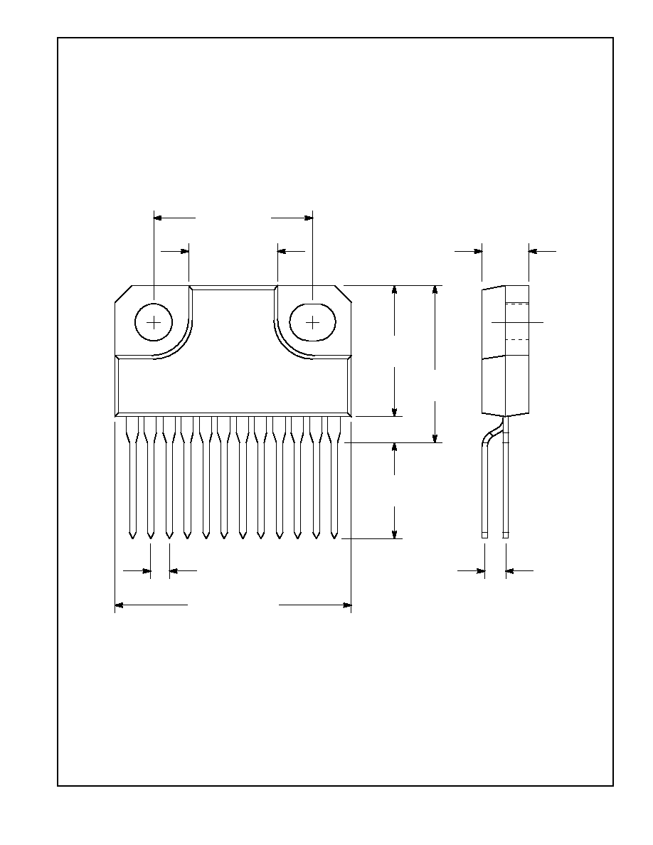
The NTE1898 and NTE1899 are dual audio power amplifiers in a 12≠Lead SIP type package de-
signed for use as high performance, car≠audio power amplifiers in consumer applications. These
devices feature high power, low distortion, and low noise along with various types of protection cir-
cuits. The NTE1899 is a mirror image pin≠out of the NTE1898 allowing for easier design of PC boards
when used in BTL≠stereo applications.
Features:
D
High Power:
P
OUT
= 22W (Typ) @ V
CC
= 14.4V, f = 1kHz, THD = 10%, R
L
= 4
(BTL)
P
OUT
= 5.8W/Ch (Typ) @ V
CC
= 13.2V, f = 1kHz, THD = 10%, R
L
= 4
(Dual)
D
Low Distortion:
THD = 0.03% (Typ) @ V
CC
= 14.4V, f = 1kHz, P
OUT
= 4W, R
L
= 4
, G
V
= 40dB (BTL)
THD = 0.06% (Typ) @ V
CC
= 13.2V, f = 1kHz, P
OUT
= 1W, R
L
= 4
, G
V
= 52dB (Dual)
D
Low Noise:
V
NO
= 0.14mV
rms
(Typ) @ V
CC
= 13.2V, R
L
= 4
, G
V
= 40dB, R
g
= 0, DIN Noise: DIN45405
V
NO
= 0.7mV
rms
(Typ) @ V
CC
= 13.2V, R
L
= 4
, G
V
= 52dB, BW = 20Hz to 20kHz (Dual)
D
Protector Circuit:
Thermal Shut Down, Overvoltage, OUT≠V
CC
Short, OUT≠GND Short, OUT≠OUT Short
Absolute Maximum Ratings: (T
A
= +25
∞
C unless othrwise specified)
Peak Supply Voltage (0.2sec), V
CC
surge
45V
. . . . . . . . . . . . . . . . . . . . . . . . . . . . . . . . . . . . . . . . . . . . . .
DC Supply Voltage, V
CC
DC
25V
. . . . . . . . . . . . . . . . . . . . . . . . . . . . . . . . . . . . . . . . . . . . . . . . . . . . . . . . . .
Operating Supply Voltage, V
CC
opr
18V
. . . . . . . . . . . . . . . . . . . . . . . . . . . . . . . . . . . . . . . . . . . . . . . . . . . .
Peak Output Current, I
O
peak
4.5A
. . . . . . . . . . . . . . . . . . . . . . . . . . . . . . . . . . . . . . . . . . . . . . . . . . . . . . .
Power Dissipation, P
D
25W
. . . . . . . . . . . . . . . . . . . . . . . . . . . . . . . . . . . . . . . . . . . . . . . . . . . . . . . . . . . . .
Operating Temperature Range, T
opr
≠30
∞
to +85
∞
C
. . . . . . . . . . . . . . . . . . . . . . . . . . . . . . . . . . . . . . . . .
Storage Temperature Range, T
stg
≠55
∞
to +150
∞
C
. . . . . . . . . . . . . . . . . . . . . . . . . . . . . . . . . . . . . . . . . .