NTE1908
Integrated Circuit
Positive 3 Terminal Voltage Regulator,
24V, 100mA
Description:
The NTE1908 voltage regulator is an inexpensive, easy≠to≠use device in a TO92 type package suitable
for a multitude of applications that require a regulated supply of up to 100mA. This device features internal
current limiting and thermal shutdown making the NTE1908 remarkably rugged. No external components
are required in many applications.
The NTE1908 offers a substantial performance advantage over the traditional zener diode≠resistor
combination, as output impedance and quiescent current are substantially reduced.
Features:
D
Low Cost
D
±
5% Tolerance
D
Internal Short≠Circuit Current Limiting
D
Internal Thermal Overload Protection
D
No External Components Required
D
Complementary to NTE1909 Negative Regulator
Absolute Maximum Ratings: (T
A
= +25
∞
C unless otherwise specified)
Input Voltage, V
I
40V
. . . . . . . . . . . . . . . . . . . . . . . . . . . . . . . . . . . . . . . . . . . . . . . . . . . . . . . . . . . . . . . . . . .
Operating Junction Temperature Range, T
J
0
∞
to +150
∞
C
. . . . . . . . . . . . . . . . . . . . . . . . . . . . . . . . . . . .
Storage Junction Temperature Range, T
stg
≠65
∞
to +150
∞
C
. . . . . . . . . . . . . . . . . . . . . . . . . . . . . . . . . .
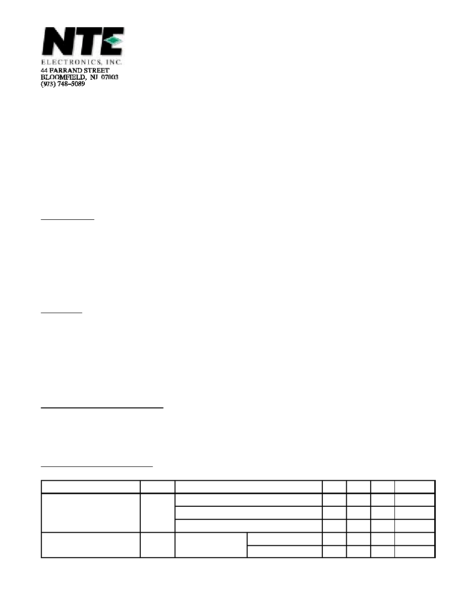
Electrical Characteristics: (V
I
= 33V, I
O
= 40mA, C
I
= 0.33
µ
F, C
O
= 0.1
µ
F, 0
∞
< T
J
< +125
∞
C
unless otherwise specified)
Parameter
Symbol
Test Conditions
Min
Typ
Max
Unit
Output Voltage
V
O
T
J
= +25
∞
C
22.1
24.0
25.9
V
28V
V
I
38V, 1mA
I
O
40mA
21.6
≠
26.4
V
28V
V
I
33V, 1mA
I
O
70mA
21.6
≠
26.4
V
Line Regulation
Reg
line
T
J
= +25
∞
C,
27.5V
V
I
38V
≠
35
350
mV
I
O
= 40mA
28V
V
I
80V
≠
30
300
mV
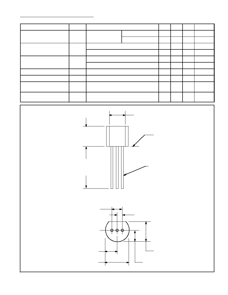
Electrical Characteristics (Cont'd): (V
I
= 33V, I
O
= 40mA, C
I
= 0.33
µ
F, C
O
= 0.1
µ
F,
0
∞
< T
J
< +125
∞
C unless otherwise specified)
Parameter
Symbol
Test Conditions
Min
Typ
Max
Unit
Load Regulation
Reg
load
T
J
= +25
∞
C
1mA
I
O
100mA
≠
40
200
mV
1mA
I
O
40mA
≠
20
100
mV
Input Bias Current
I
IB
T
J
= +25
∞
C
≠
3.1
6.5
mA
T
J
= +125
∞
C
≠
≠
6.0
mA
Input Bias Current Change
I
IB
28V
V
I
38V
≠
≠
1.5
mA
1mA
I
O
40mA
≠
≠
0.2
mA
Output Noise Voltage
V
n
T
A
= +25
∞
C, 10Hz
f
100kHz
≠
200
≠
µ
V
Long≠Term Stability
V
O
/
t
≠
56
≠
mV/1kHrs
Ripple Rejection
RR
I
O
= 40mA, f = 120Hz, 29V
V
I
35V,
T
J
= +25
∞
C
30
43
≠
dB
Input≠Output Voltage
Differential
V
I
/V
O
T
J
= +25
∞
C
≠
1.7
≠
V
V
OUT
GND
V
IN
.135 (3.45) Min
Seating Plane
.021 (.445) Dia Max
.210
(5.33)
Max
.500
(12.7)
Min
.050 (1.27)
.165 (4.2) Max
.105 (2.67) Max
.100 (2.54)
.105 (2.67) Max
.205 (5.2) Max