NTE2011/NTE2012/NTE2013/NTE2014/NTE2015
Integrated Circuit
7нChannel Darlington Array/Driver
Description:
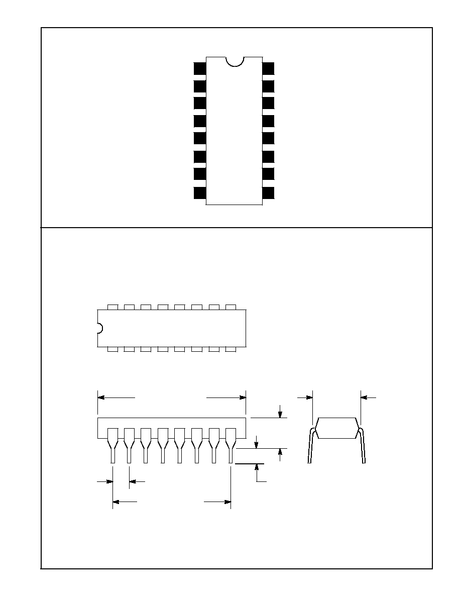
The NTE2011 through NTE2015 are highнvoltage, highнcurrent Darlington arrays in a 16нLead DIP
type package and are comprised of seven silicon NPN Darlington pairs on a common monolithic sub-
strate. All units have openнcollector outputs and integral diodes for inductive load transient suppres-
sion.
Peak inrush currents to 600mA (NTE2011, NTE2013, NTE2014) or 750mA (NTE2012, NTE2015) are
permissible, making them ideal for driving tungstun filament lamps.
The NTE2011 is a general purpose array that may be used with standard biнpolar digital logic using
external current limiting, or with most PMOS or CMOS directly. This device is pinned with outputs
opposite inputs to facilitate printed wiring board layouts.
The NTE2012 is designed for use with 14V to 25V PMOS devices. Each input has a Zener diode and
resistor in series to limit the input current to a safe value in that application. The Zener diode also gives
this device excellent noise immunity.
The NTE2013 has a 2.7k
series base resistor for each Darlington pair, allowing operation directly
with TTL or CMOS operating at a supply voltage of 5V. This device will handle numerous interface
needs н particularly those beyond the capabilities of standard logic buffers.
The NTE2014 has a 10.5k
series input resistor that permits operation directly from CMOS or PMOS
outputs utilizing supply voltages of 6V to 15V. The required input current is below that of the NTE2013,
while the required input voltage is less than that required by the NTE2012.
The NTE2015 is designed for use with standard TTL and Schottky TTL, with which higher output cur-
rents are required and loading of the logic output is not a concern. This device will sink a minimum
of 350mA when driven from a "totem pole" logic output.
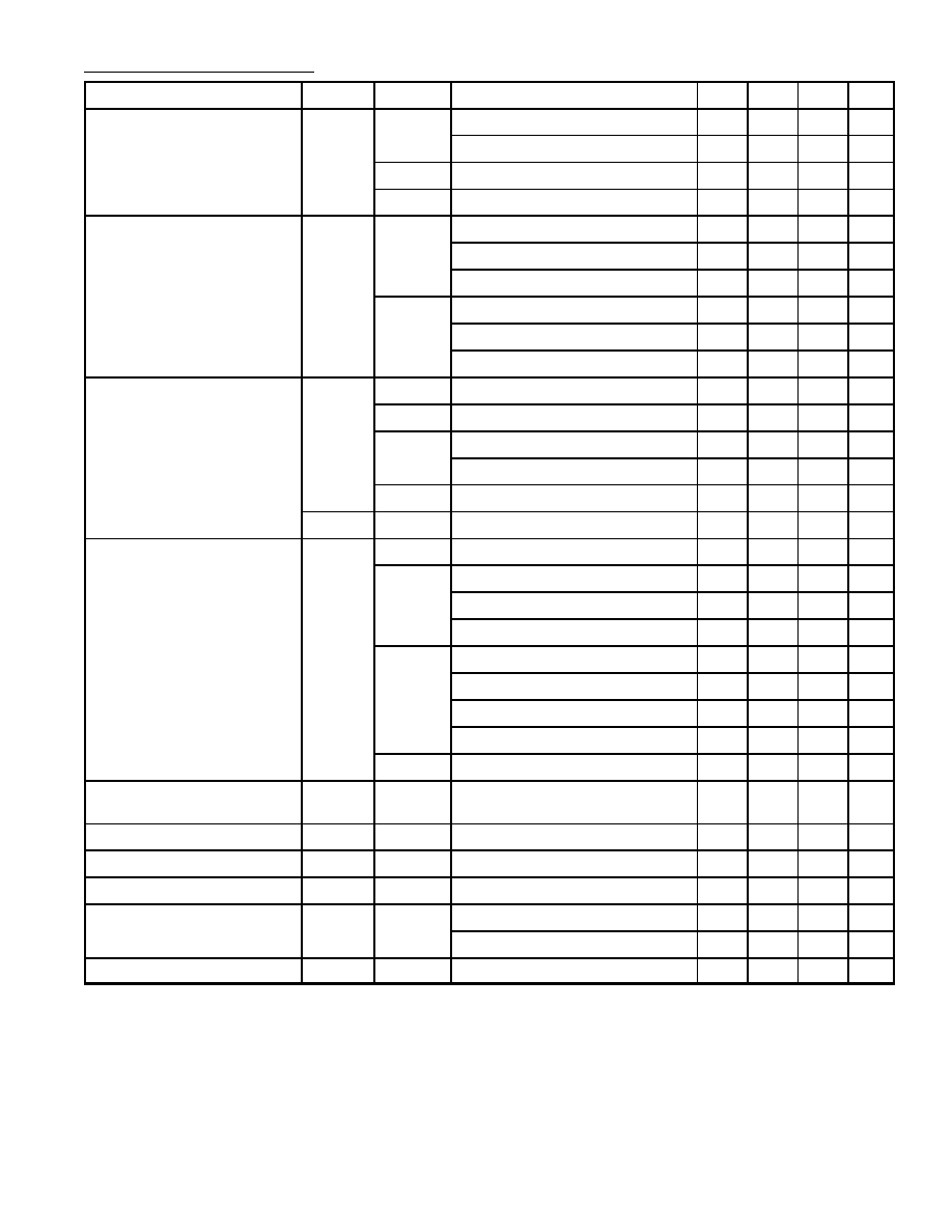
Absolute Maximum Ratings: (T
A
= +25
░
C for any one Darlington pair unless otherwise specified)
Output Voltage, V
CE
50V
. . . . . . . . . . . . . . . . . . . . . . . . . . . . . . . . . . . . . . . . . . . . . . . . . . . . . . . . . . . . . . . .
Input Voltage, V
IN
NTE2012, NTE2013, NTE2014
30V
. . . . . . . . . . . . . . . . . . . . . . . . . . . . . . . . . . . . . . . . . . . . . . . .
NTE2015
15V
. . . . . . . . . . . . . . . . . . . . . . . . . . . . . . . . . . . . . . . . . . . . . . . . . . . . . . . . . . . . . . . . . . . .
Continuous Collector Current. I
C
NTE2011, NTE2013, NTE2014
500mA
. . . . . . . . . . . . . . . . . . . . . . . . . . . . . . . . . . . . . . . . . . . . .
NTE2012, NTE2015
600mA
. . . . . . . . . . . . . . . . . . . . . . . . . . . . . . . . . . . . . . . . . . . . . . . . . . . . . . .
Continuous Input Current, I
IN
25mA
. . . . . . . . . . . . . . . . . . . . . . . . . . . . . . . . . . . . . . . . . . . . . . . . . . . . . .
Power Dissipation, P
D
One Darlington Pair
1W
. . . . . . . . . . . . . . . . . . . . . . . . . . . . . . . . . . . . . . . . . . . . . . . . . . . . . . . . . .
Total Device (Note 1)
2W
. . . . . . . . . . . . . . . . . . . . . . . . . . . . . . . . . . . . . . . . . . . . . . . . . . . . . . . . .
Operating Ambient Temperature Range, T
A
н20
░
to +85
░
C
. . . . . . . . . . . . . . . . . . . . . . . . . . . . . . . . . . .
Storage Temperature Range, T
stg
н55
░
to +150
░
C
. . . . . . . . . . . . . . . . . . . . . . . . . . . . . . . . . . . . . . . . . .
Note 1. The NTE2015 is a discontinued device and no longer available.
Note 2. Derate at the rate of 16.6mW/
░
C above +25
░
C.
Note 3. Under normal operating conditions, these devices will sustain 350mA per output with
V
CE(sat)
= 1.6V at +70
░
C with a pulse width of 20ms and a duty cycle of 34%.