
NTE2345 (NPN) & NTE2346 (PNP)
Silicon Complementary Transistors
General Purpose Darlington, Power Amplifier
Description:
The NTE2345 (NPN) and NTE2346 (PNP) are silicon complementary Darlington transistors in an
SOTÙ82 type package designed for use in audio output stages and general amplifier and switching
applications..
Features:
D
High DC Current Gain:
h
FE
= 750 (Min) @ I
C
= 3A, V
CE
= 3V
D
Junction Temperature to +150
¯
C
Absolute Maximum Ratings:
CollectorÙEmitter Voltage, V
CEO
120V
. . . . . . . . . . . . . . . . . . . . . . . . . . . . . . . . . . . . . . . . . . . . . . . . . . . . .
CollectorÙBase Voltage, V
CBO
120V
. . . . . . . . . . . . . . . . . . . . . . . . . . . . . . . . . . . . . . . . . . . . . . . . . . . . . .
EmitterÙBase Voltage, V
EBO
5V
. . . . . . . . . . . . . . . . . . . . . . . . . . . . . . . . . . . . . . . . . . . . . . . . . . . . . . . . . .
Collector Current, I
C
Continuous
6A
. . . . . . . . . . . . . . . . . . . . . . . . . . . . . . . . . . . . . . . . . . . . . . . . . . . . . . . . . . . . . . . . . . .
Peak (t
p
10ms,
0.1)
10A
. . . . . . . . . . . . . . . . . . . . . . . . . . . . . . . . . . . . . . . . . . . . . . . . . . . . . .
Base Current, I
B
150mA
. . . . . . . . . . . . . . . . . . . . . . . . . . . . . . . . . . . . . . . . . . . . . . . . . . . . . . . . . . . . . . . .
Total Power Dissipation (T
C
= +25
¯
C), P
D
60W
. . . . . . . . . . . . . . . . . . . . . . . . . . . . . . . . . . . . . . . . . . . .
Junction Temperature, T
J
+150
¯
C
. . . . . . . . . . . . . . . . . . . . . . . . . . . . . . . . . . . . . . . . . . . . . . . . . . . . . . . . .
Storage Temperature Range, T
stg
Ù65
¯
to +150
¯
C
. . . . . . . . . . . . . . . . . . . . . . . . . . . . . . . . . . . . . . . . . .
Thermal Resistance, JunctionÙtoÙCase, R
thJC
2.08K/W
. . . . . . . . . . . . . . . . . . . . . . . . . . . . . . . . . . . . .
Thermal Resistance, JunctionÙtoÙAmbient, R
thJA
100K/W
. . . . . . . . . . . . . . . . . . . . . . . . . . . . . . . . . . .
Electrical Characteristics: (T
J
= +25
¯
C unless otherwise specified)
Parameter
Symbol
Test Conditions
Min
Typ
Max
Unit
Collector Cutoff Current
I
CBO
I
E
= 0, V
CBO
= 120V
Ù
Ù
0.2
mA
I
E
= 0, V
CBO
= 120V, T
J
= +150
¯
C
Ù
Ù
2mA
mA
I
CEO
I
B
= 0, V
CEO
= 60V
Ù
Ù
0.5
mA
Emitter Cutoff Current
I
EBO
I
C
= 0, V
EBO
= 5V
Ù
Ù
5
mA
DC Current Gain
h
FE
I
C
= 500mA, V
CEO
= 3V, Note 1
Ù
2700
Ù
I
C
= 3A, V
CEO
= 3V, Note 1
750
Ù
Ù
I
C
= 6A, V
CEO
= 3V, Note 1
Ù
400
Ù
Note 1. Pulse Test: Pulse Width
300
ç
s, Duty Cycle
2%.
Electrical Characteristics (Cont'd): (T
J
= +25
¯
C unless otherwise specified)
Parameter
Symbol
Test Conditions
Min
Typ
Max
Unit
BaseÙEmitter Voltage
V
BE
I
C
= 3A, V
CEO
= 3V, Note 2
2.5
Ù
Ù
V
CollectorÙEmitter Saturation Voltage
V
CE(sat)
I
C
= 3A, I
B
= 12mA
2.0
Ù
Ù
V
SmallÙSignal Current Gain
h
fe
I
C
= 3A, V
CEO
= 3V, f = 1MHz
10
Ù
Ù
CutÙOff Frequency
f
hfe
I
C
= 3A, V
CEO
= 3V
Ù
100
Ù
kHz
Diode, Forward Voltage
V
F
I
F
= 3A
Ù
1.8
Ù
V
Second Breakdown Collector Current
NonÙRepetitive, without Heatsink
I
(SB)
V
CEO
= 60V, t
p
= 25ms
1
Ù
Ù
A
TurnÙOn Time
t
on
I
C(on)
= 3A, I
B(on)
= I
B(off)
= 12mA
Ù
1
2
ç
s
TurnÙOff Time
t
off
I
C(on)
= 3A, I
B(on)
= I
B(off)
= 12mA
Ù
5
10
ç
s
Note 2. V
BE
decreases by about 3.8mV/K with increasing temperature.
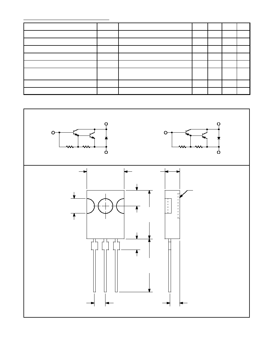
Schematic Diagram
NPN
PNP
B
C
E
B
C
E
B
C
E
.118 (3.0)
Min
.147
(3.75)
.100 (2.54)
.090 (2.29)
.047 (1.2)
.307 (7.8)
Max
.100 (2.54)
See Note
.437
(11.1)
Max
.602
(15.3)
Min
Note: Collector connected to metal part of mounting surface.