NTE2375
MOSFET
NÙCh, Enhancement Mode
High Speed Switch
Features:
D
Dynamic dv/dt Rating
D
Repetitive Avalanche Rated
D
Isolated Central Mounting Hole
D
Fast Switching
D
Ease of Paralleling
D
Simple Drive Requirements
Absolute Maximum Ratings:
Continuous Drain Current (V
GS
= 10V), I
D
T
C
= +25
¯
C
41A
. . . . . . . . . . . . . . . . . . . . . . . . . . . . . . . . . . . . . . . . . . . . . . . . . . . . . . . . . . . . . . . . . .
T
C
= +100
¯
C
29A
. . . . . . . . . . . . . . . . . . . . . . . . . . . . . . . . . . . . . . . . . . . . . . . . . . . . . . . . . . . . . . . . .
Pulsed Drain Current (Note 1), I
DM
120A
. . . . . . . . . . . . . . . . . . . . . . . . . . . . . . . . . . . . . . . . . . . . . . . . . .
Power Dissipation (T
C
= +25
¯
C), P
D
230W
. . . . . . . . . . . . . . . . . . . . . . . . . . . . . . . . . . . . . . . . . . . . . . . .
Derate Linearly Above 25
¯
C
1.5W/
¯
C
. . . . . . . . . . . . . . . . . . . . . . . . . . . . . . . . . . . . . . . . . . . . . . .
GateÙtoÙSource Voltage, V
GS
Ý
20V
. . . . . . . . . . . . . . . . . . . . . . . . . . . . . . . . . . . . . . . . . . . . . . . . . . . . . .
Single Pulse Avalanche Energy (Note 2), E
AS
830mJ
. . . . . . . . . . . . . . . . . . . . . . . . . . . . . . . . . . . . . . .
Avalanche Current (Note 1), I
AR
41A
. . . . . . . . . . . . . . . . . . . . . . . . . . . . . . . . . . . . . . . . . . . . . . . . . . . . . .
Repetitive Avalanche Energy (Note 1), E
AR
19mJ
. . . . . . . . . . . . . . . . . . . . . . . . . . . . . . . . . . . . . . . . . .
Peak Diode Recovery dv/dt (Note 3), dv/dt
5.5V/ns
. . . . . . . . . . . . . . . . . . . . . . . . . . . . . . . . . . . . . . . . .
Operating Junction Temperature Range, T
J
Ù55
¯
to +175
¯
C
. . . . . . . . . . . . . . . . . . . . . . . . . . . . . . . . . .
Storage Temperature Range, T
stg
Ù55
¯
to +175
¯
C
. . . . . . . . . . . . . . . . . . . . . . . . . . . . . . . . . . . . . . . . . .
Lead Temperature (During Soldering, 1.6mm from case for 10sec), T
L
+300
¯
C
. . . . . . . . . . . . . . . . .
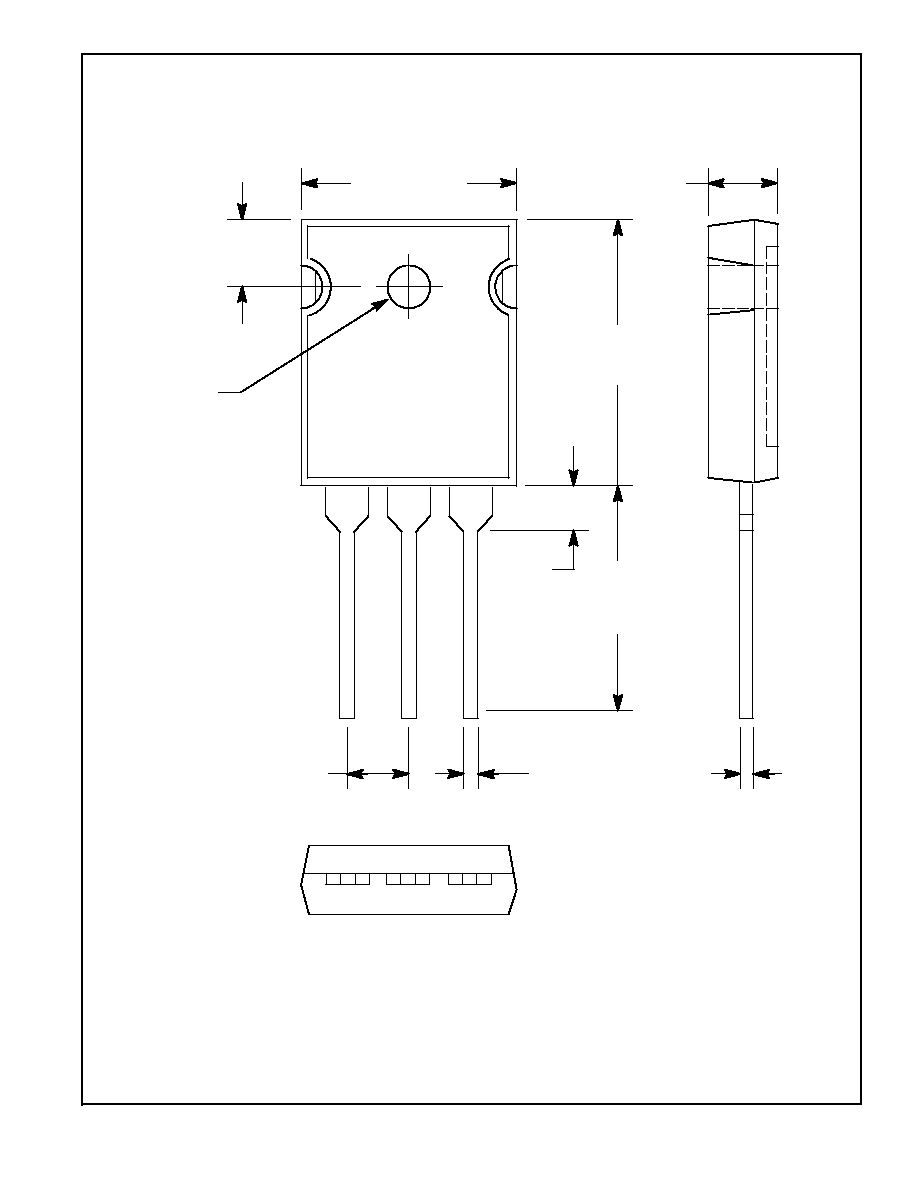
Mounting Torque (6Ù32 or M3 Screw)
10 lbf
in (1.1N
m)
. . . . . . . . . . . . . . . . . . . . . . . . . . . . . . . . . . . .
Thermal Resistance, JunctionÙtoÙCase, R
thJC
0.65
¯
C/W
. . . . . . . . . . . . . . . . . . . . . . . . . . . . . . . . . . . .
Thermal Resistance, JunctionÙtoÙAmbient, R
thJA
40
¯
C/W
. . . . . . . . . . . . . . . . . . . . . . . . . . . . . . . . . . .
Typical Thermal Resistance, CaseÙtoÙSink (Flat, Greased Surface), R
thCS
0.24
¯
C/W
. . . . . . . . . . .
Note 1. Repetitive rating; pulse width limited by maximum junction temperature.
Note 2. V
DD
= 25V, starting T
J
= +25
¯
C, L = 740
ç
H, R
G
= 25
, I
AS
= 41A
Note 3. I
SD
41A, di/dt
300A/
ç
s, V
DD
V
(BR)DSS
, T
J
+175
¯
C
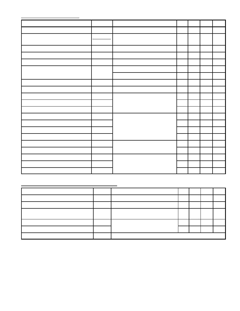
Electrical Characteristics: (T
J
= +25
¯
C unless otherwise specified)
Parameter
Symbol
Test Conditions
Min
Typ
Max
Unit
DrainÙtoÙSource Breakdown Voltage
V
(BR)DSS
V
GS
= 0V, I
D
= 250
ç
A
100
Ù
Ù
V
Breakdown Voltage Temp. Coefficient
V
(BR)DSS
T
J
Reference to +25
¯
C, I
D
= 1mA
Ù
0.14
Ù
V/
¯
C
Static DrainÙtoÙSource OnÙResistance
R
DS(on)
V
GS
= 10V, I
D
= 25A, Note 4
Ù
Ù
0.055
Gate Threshold Voltage
V
GS(th)
V
DS
= V
GS
, I
D
= 250
ç
A
2.0
Ù
4.0
V
Forward Transconductance
g
fs
V
DS
= 25V, I
D
= 25A, Note 4
13
Ù
Ù
mhos
DrainÙtoÙSource Leakage Current
I
DSS
V
DS
= 100V, V
GS
= 0V
Ù
Ù
25
ç
A
V
DS
= 80V, V
GS
= 0V, T
J
= +150
¯
C
Ù
Ù
250
ç
A
GateÙtoÙSource Forward Leakage
I
GSS
V
GS
= 20V
Ù
Ù
100
nA
GateÙtoÙSource Reverse Leakage
I
GSS
V
GS
= Ù20V
Ù
Ù
Ù100
nA
Total Gate Charge
Q
g
I
D
= 41A, V
DS
= 80V, V
GS
= 10V,
Ù
Ù
140
nC
GateÙtoÙSource Charge
Q
gs
Note 4
Ù
Ù
29
nC
GateÙtoÙDrain ("Miller") Charge
Q
gd
Ù
Ù
68
nC
TurnÙOn Delay Time
t
d(on)
V
DD
= 50V, I
D
= 41A, R
G
= 6.2
,
Ù
16
Ù
ns
Rise Time
t
r
R
D
= 1.2
, Note 4
Ù
120
Ù
ns
TurnÙOff Delay Time
t
d(off)
Ù
60
Ù
ns
Fall Time
t
f
Ù
81
Ù
ns
Internal Drain Inductance
L
D
Between lead, .250in. (6.0) mm from
Ù
5.0
Ù
nH
Internal Source Inductance
L
S
package and center of die contact
Ù
13.0
Ù
nH
Input Capacitance
C
iss
V
GS
= 0V, V
DS
= 25V, f = 1MHz
Ù
2800
Ù
pF
Output Capacitance
C
oss
Ù
1100
Ù
pF
Reverse Transfer Capaticance
C
rss
Ù
280
Ù
pF
SourceÙDrain Ratings and Characteristics:
Parameter
Symbol
Test Conditions
Min
Typ
Max
Unit
Continuous Source Current (Body Diode)
I
S
Ù
Ù
41
A
Pulsed Source Current (Body Diode)
I
SM
Note 1
Ù
Ù
160
A
Diode Forward Voltage
V
SD
T
J
= +25
¯
C, I
S
= 41A, V
GS
= 0V,
Note 4
Ù
Ù
2.5
V
Reverse Recovery Time
t
rr
T
J
= +25
¯
C, I
F
= 41A,
Ù
220
330
ns
Reverse Recovery Charge
Q
rr
di/dt = 100A/
ç
s, Note 4
Ù
1.9
2.9
ç
C
Forward TurnÙOn Time
t
on
Intrinsic turnÙon time is neglegible (turnÙon is dominated by L
S
+L
D
)
Note 1. Repetitive rating; pulse width limited by maximum junction temperature.
Note 4. Pulse width
300
ç
s; duty cycle
2%.