
NTE2390
MOSFET
NÙChannel Enhancement Mode,
High Speed Switch
Description:
The NTE2390 is an NÙChannel Enhancement Mode Power MOS Field Effect Transistor in a TO220
type package designed for low voltage, high speed power switching applications such as switching
regulators, converters, solenoid, and relay drivers.
Features:
D
Silicon Gate for Fast Switching Speeds
D
I
DSS
, V
DC(on)
, V
GS(th)
, and SOA Specified at Elevated Temperatures.
D
Rugged Ù SOA is Power Dissipation Limited
D
SourceÙtoÙDrain Diode Characterized for Use With Inductive Loads
Absolute Maximum Ratings:
DrainÙSource Voltage, V
DSS
60V
. . . . . . . . . . . . . . . . . . . . . . . . . . . . . . . . . . . . . . . . . . . . . . . . . . . . . . . . .
DrainÙGate Voltage (R
GS
= 1M
), V
DGR
60V
. . . . . . . . . . . . . . . . . . . . . . . . . . . . . . . . . . . . . . . . . . . . . .
GateÙSource Voltage, V
GS
Ý
20V
. . . . . . . . . . . . . . . . . . . . . . . . . . . . . . . . . . . . . . . . . . . . . . . . . . . . . . . . .
Drain Current, I
D
Continuous
12A
. . . . . . . . . . . . . . . . . . . . . . . . . . . . . . . . . . . . . . . . . . . . . . . . . . . . . . . . . . . . . . . . . .
Pulsed
30A
. . . . . . . . . . . . . . . . . . . . . . . . . . . . . . . . . . . . . . . . . . . . . . . . . . . . . . . . . . . . . . . . . . . . . .
Total Power Dissipation (T
C
= +25
¯
C), P
D
75W
. . . . . . . . . . . . . . . . . . . . . . . . . . . . . . . . . . . . . . . . . . . .
Derate Above 25
¯
C
0.6W/
¯
C
. . . . . . . . . . . . . . . . . . . . . . . . . . . . . . . . . . . . . . . . . . . . . . . . . . . . . . .
Operating Junction Temperature Range, T
J
Ù65
¯
to +150
¯
C
. . . . . . . . . . . . . . . . . . . . . . . . . . . . . . . . . .
Storage Temperature Range, T
stg
Ù65
¯
to +150
¯
C
. . . . . . . . . . . . . . . . . . . . . . . . . . . . . . . . . . . . . . . . . .
Maximum Thermal Resistance, JunctionÙtoÙCase, R
thJC
1.67
¯
C/W
. . . . . . . . . . . . . . . . . . . . . . . . . . .
Maximum Thermal Resistance, JunctionÙtoÙAmbient, R
thJA
30
¯
C/W
. . . . . . . . . . . . . . . . . . . . . . . . .
Maximum Lead Temperature (During soldering), T
L
+275
¯
C
. . . . . . . . . . . . . . . . . . . . . . . . . . . . . . . . . .
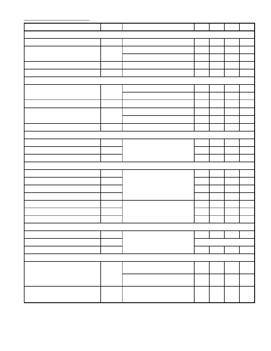
Electrical Characteristics: (T
C
= +25
¯
C unless otherwise specified)
Parameter
Symbol
Test Conditions
Min
Typ
Max
Unit
OFF Characteristics
DrainÙSource Breakdown Voltage
V
(BR)DSS
I
D
= 0.25mA, V
GS
= 0
60
Ù
Ù
V
ZeroÙGate Voltage Drain Current
I
DSS
V
GS
= 0, V
DS
= Max Rating
Ù
Ù
0.2
mA
V
GS
= 0, V
DS
= 48V, T
J
= +125
¯
C
Ù
Ù
1.0
mA
GateÙBody Leakage Current, Forward
I
GSSF
V
DS
= 0, V
GSF
= 20V
Ù
Ù
100
nA
GateÙBody Leakage Current, Reverse
I
GSSR
V
DS
= 0, V
GSR
= 20V
Ù
Ù
100
nA
ON Characteristics (Note 1)
Gate Threshold Voltage
V
GS(th)
V
DS
= V
GS
, I
D
= 1mA
2.0
Ù
4.5
V
V
DS
= V
GS
, I
D
= 1mA, T
J
= +100
¯
C
1.5
Ù
4.0
V
Static DrainÙSource On Resistance
r
DS(on)
V
GS
= 10V, I
D
= 6A
Ù
Ù
0.2
DrainÙSource ONÙVoltage
V
DS(on)
V
GS
= 10V, I
D
= 12A
Ù
Ù
3.0
V
V
GS
= 10V, I
D
= 6A, T
J
= 100
¯
C
Ù
Ù
2.8
V
Forward Transconductance
g
fs
V
DS
= 15V, I
D
= 6A
4
Ù
Ù
mhos
Dynamic Characteristics
Input Capactiance
C
iss
V
DS
= 25V, V
GS
= 0,
Ù
Ù
400
pf
Output Capacitance
C
oss
f = 1MHz
Ù
Ù
300
pf
Reverse Transfer Capactiance
C
rss
Ù
Ù
100
pf
Switching Characteristics (T
J
= +100
¯
C, Note 1)
TurnÙOn Time
t
d(on)
V
DD
= 25V, I
D
= 0.5 Rated I
D
,
Ù
Ù
60
ns
Rise Time
t
r
R
gen
= 50
Ù
Ù
160
ns
TurnÙOff Delay Time
t
d(off)
Ù
Ù
80
ns
Fall Time
t
f
Ù
Ù
110
ns
Total Gate Charge
Q
g
V
DS
= 48V, V
GS
= 10V,
Ù
13
26
nC
GateÙSource Charge
Q
gs
I
D
= Rated I
D
Ù
6
Ù
nC
GateÙDrain Charge
Q
gd
Ù
7
Ù
nC
Source Drain Diode Characteristics (Note 1)
Forward ON Voltage
V
SD
I
S
= Rated I
D
, V
GS
= 0
Ù
1.8
3.2
V
Forward TurnÙOn Time
t
on
Limited by stray inductance
Reverse Recovery Time
t
rr
Ù
300
Ù
ns
Internal Package Inductance
Internal Drain Inductance
L
d
Measured from the contact screw
on tab to center of die
Ù
3.5
Ù
nH
Measured from the drain lead 0.25"
from package to center of die
Ù
4.5
Ù
nH
Internal Source Inductance
L
s
Measured from the source lead
0.25" from package to source bond
pad
Ù
7.5
Ù
nH
Note 1. Pulse test: Pulse width
300
ç
s, Duty cycle
2%.
