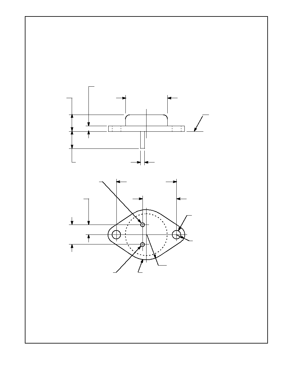
NTE2392
MOSFET
N≠Channel Enhancement Mode,
High Speed Switch
Description:
The NTE2392 is an N≠Channel Enhancement Mode Power MOS Field Effect Transistor. Easy drive
and very fast switching times make this device ideal for high speed switching applications. Typical
applications include switching mode power supplies, uninterruptible power supplies, and motor
speed control.
Features:
D
Fast Switching
D
Low Drive Current
D
Ease of Paralleling
D
No Second Breakdown
D
Excellent Temperature Stability
Absolute Maximum Ratings:
Drain≠Source Voltage (Note 1), V
DS
100V
. . . . . . . . . . . . . . . . . . . . . . . . . . . . . . . . . . . . . . . . . . . . . . . . .
Drain≠Gate Voltage (R
GS
= 20k
,
Note 1), V
DGR
100V
. . . . . . . . . . . . . . . . . . . . . . . . . . . . . . . . . . . . . .
Gate≠Source Voltage, V
GS
±
20V
. . . . . . . . . . . . . . . . . . . . . . . . . . . . . . . . . . . . . . . . . . . . . . . . . . . . . . . . .
Pulsed Drain Current (Note 3), I
DM
160A
. . . . . . . . . . . . . . . . . . . . . . . . . . . . . . . . . . . . . . . . . . . . . . . . . .
Clamped Inductive Current (L = 100
µ
H), I
LM
160A
. . . . . . . . . . . . . . . . . . . . . . . . . . . . . . . . . . . . . . . . . .
Continuous Drain Current, I
D
T
C
= +25
∞
C
40A
. . . . . . . . . . . . . . . . . . . . . . . . . . . . . . . . . . . . . . . . . . . . . . . . . . . . . . . . . . . . . . . . . .
T
C
= +100
∞
C
25A
. . . . . . . . . . . . . . . . . . . . . . . . . . . . . . . . . . . . . . . . . . . . . . . . . . . . . . . . . . . . . . . . .
Total Dissipation (T
C
= +25
∞
C), P
tot
150W
. . . . . . . . . . . . . . . . . . . . . . . . . . . . . . . . . . . . . . . . . . . . . . . . .
Derate Above 25
∞
C
1.2W/
∞
C
. . . . . . . . . . . . . . . . . . . . . . . . . . . . . . . . . . . . . . . . . . . . . . . . . . . . . . .
Operating Junction Temperature Range, T
J
≠55
∞
to +150
∞
C
. . . . . . . . . . . . . . . . . . . . . . . . . . . . . . . . . .
Storage Temperature Range, T
stg
≠55
∞
to +150
∞
C
. . . . . . . . . . . . . . . . . . . . . . . . . . . . . . . . . . . . . . . . . .
Lead Temperature (During Soldering, 0.063 in. (1.6mm) from case, 10sec), T
L
+300
∞
C
. . . . . . . . . .
Maximum Thermal Resistance, Junction≠to≠Case, R
thJC
0.83
∞
C/W
. . . . . . . . . . . . . . . . . . . . . . . . . . .
Typical Thermal Resistance, Case≠to≠Sink (Note 4), R
thCS
0.1
∞
C/W
. . . . . . . . . . . . . . . . . . . . . . . . . .
Maximum Thermal Resistance, Junction≠to≠Ambient, R
thJA
30
∞
C/W
. . . . . . . . . . . . . . . . . . . . . . . . .
Note 1. T
J
= +25
∞
to +150
∞
C
Note 2. Pulse test: Pulse Width
300
µ
s, Duty Cycle
2%.
Note 3. Repetitive Rating: Pulse width limited by maximum junction temperature.
Note 4. Mounting surface flat, smooth, and greased.
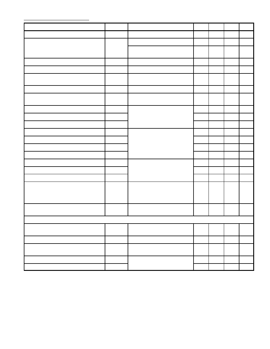
Electrical Characteristics: (T
C
= +25
∞
C unless otherwise specified)
Parameter
Symbol
Test Conditions
Min
Typ
Max
Unit
Drain≠Source Breakdown Voltage
V
(BR)DSS
I
D
= 250
µ
A, V
GS
= 0
100
≠
≠
V
Zero≠Gate Voltage Drain Current
I
DSS
V
GS
= 0, V
DS
= 100V
≠
≠
250
µ
A
V
GS
= 0, V
DS
= 80V,
T
C
= +125
∞
C
≠
≠
1000
µ
A
Gate≠Body Leakage Current
I
GSS
V
DS
= 0, V
GS
=
±
20V
≠
≠
±
100
nA
Gate Threshold Voltage
V
GS(th)
V
DS
= V
GS
, I
D
= 250
µ
A
2
≠
4
V
On≠State Drain Current
I
D(on)
V
DS
> I
D(on)
x R
DS(on) max
,
V
GS
= 10V, Note 2
40
≠
≠
A
Static Drain≠Source On Resistance
R
DS(on)
V
GS
= 10V, I
D
= 20A, Note 2
≠
0.045
0.055
W
Forward Transconductance
g
fs
V
DS
> I
D(on)
x R
DS(on) max
,
I
D
= 20A, Note 2
9
11
≠
mho
Input Capactiance
C
iss
V
DS
= 25V, V
GS
= 0, f = 1MHz
≠
2000
3000
pf
Output Capacitance
C
oss
≠
1000
1500
pf
Reverse Transfer Capactiance
C
rss
≠
350
500
pf
Turn≠On Time
t
d(on)
V
DD
= 24V, I
D
= 20A, R
I
= 4.7
≠
≠
35
ns
Rise Time
t
r
≠
≠
100
ns
Turn≠Off Delay Time
t
d(off)
≠
≠
125
ns
Fall Time
t
f
≠
≠
100
ns
Total Gate Charge
Q
g
V
GS
= 10V, I
D
= 50A,
≠
63
120
nC
Gate≠Source Charge
Q
gs
V
DS
= 80V
≠
27
≠
nC
Gate≠Drain ("Miller") Charge
Q
gd
≠
36
≠
nC
Internal Drain Inductance
L
D
Measured between the contact
screw on header that is closer to
source and gate pins and center of
die
≠
5.0
≠
nH
Internal Source Inductance
L
S
Measured from the source pin,
6mm (.25 in.) from header
≠
12.5
≠
nH
Source≠Drain Diode Ratings and Characteristics
Continuous Source Current
(Body Diode)
I
S
≠
≠
40
A
Pulsed Source Current (Body Diode)
I
SM
Note 3
≠
≠
160
A
Forward ON Voltage
V
SD
I
S
= 40A, V
GS
= 0, T
J
= +25
∞
C,
Note 3
≠
≠
2.5
V
Reverse Recovery Time
t
rr
I
F
= 40A, di
F
/dt = 100A/
µ
s,
∞
≠
600
≠
ns
Reverse Recovered Charge
Q
rr
T
J
= +150
∞
C
≠
3.3
≠
µ
C
Note 2. Pulse test: Pulse Width
300
µ
s, Duty Cycle
2%.
Note 3. Repetitive Rating: Pulse width limited by maximum junction temperature.