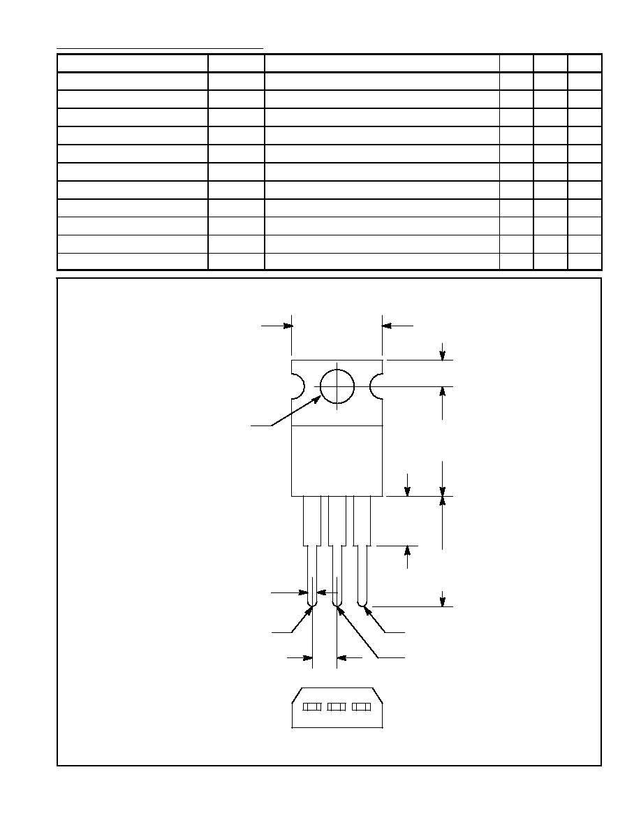
NTE5437 & NTE5438
Silicon Controlled Rectifier (SCR)
8 Amp
Description:
The NTE5437 and NTE5438 are silicon controlled rectifiers (SCR) in a TO220 type package designed
for general purpose high voltage applications where gate sensitivity is required.
Absolute Maximum Ratings: (T
A
= +25
∞
C unless otherwise specified)
Repetitive Peak Off≠State Voltage (T
J
= ≠40
∞
to +125
∞
C, R
GK
= 1k
), V
DRM
, V
RRM
NTE5437
400V
. . . . . . . . . . . . . . . . . . . . . . . . . . . . . . . . . . . . . . . . . . . . . . . . . . . . . . . . . . . . . . . . . . .
NTE5438
600V
. . . . . . . . . . . . . . . . . . . . . . . . . . . . . . . . . . . . . . . . . . . . . . . . . . . . . . . . . . . . . . . . . . .
On≠State Current (All Conducting Angles, T
C
= +85
∞
C), I
T(RMS)
8A
. . . . . . . . . . . . . . . . . . . . . . . . . . .
Average On≠State Current (Half Cycle,
= 180
∞
, T
C
= +85
∞
C), I
T(AV)
5.1A
. . . . . . . . . . . . . . . . . . . .
Non≠Repetitive On≠State Current, I
TSM
Half Cycle, 60Hz
88A
. . . . . . . . . . . . . . . . . . . . . . . . . . . . . . . . . . . . . . . . . . . . . . . . . . . . . . . . . . . . .
Half Cycle, 50Hz
80A
. . . . . . . . . . . . . . . . . . . . . . . . . . . . . . . . . . . . . . . . . . . . . . . . . . . . . . . . . . . . .
Fusing Current (t= 10ms, Half Cycle), I
2
t
32A
2
s
. . . . . . . . . . . . . . . . . . . . . . . . . . . . . . . . . . . . . . . . . . . .
Peak Reverse Gate Voltage (I
GR
= 50
µ
A), V
GRM
8V
. . . . . . . . . . . . . . . . . . . . . . . . . . . . . . . . . . . . . . . .
Peak Gate Current (10
µ
s Max), I
GM
2A
. . . . . . . . . . . . . . . . . . . . . . . . . . . . . . . . . . . . . . . . . . . . . . . . . . .
Peak Gate Dissipation (10
µ
s Max), P
GM
5W
. . . . . . . . . . . . . . . . . . . . . . . . . . . . . . . . . . . . . . . . . . . . . . .
Gate Dissipation (20ms Max), P
G(AV)
0.5W
. . . . . . . . . . . . . . . . . . . . . . . . . . . . . . . . . . . . . . . . . . . . . . . .
Oprating Junction Temperature Range, T
J
≠40
∞
to +125
∞
C
. . . . . . . . . . . . . . . . . . . . . . . . . . . . . . . . . . .
Storage Temperature Range, T
stg
≠40
∞
to +125
∞
C
. . . . . . . . . . . . . . . . . . . . . . . . . . . . . . . . . . . . . . . . . .
Lead Temperature (During Soldering, 1.6mm from case, 10sec Max), T
L
+250
∞
C
. . . . . . . . . . . . . . .
Thermal Resistance, Junction≠to≠Case, R
thJC
4K/W
. . . . . . . . . . . . . . . . . . . . . . . . . . . . . . . . . . . . . . . .
Thermal Resistance, Junction≠to≠Ambient, R
thJA
60K/W
. . . . . . . . . . . . . . . . . . . . . . . . . . . . . . . . . . . .
Electrical Characteristics: (T
A
= +25
∞
C unless otherwise specified)
Parameter
Symbol
Test Conditions
Min
Max
Unit
Off≠State Leakage Current
I
DRM
, I
RRM
V
DRM
+ V
RRM
= Rated Voltage,
T
J
= +125
∞
C
≠
0.5
mA
R
GK
= 1k
T
J
= +25
∞
C
≠
5.0
µ
A