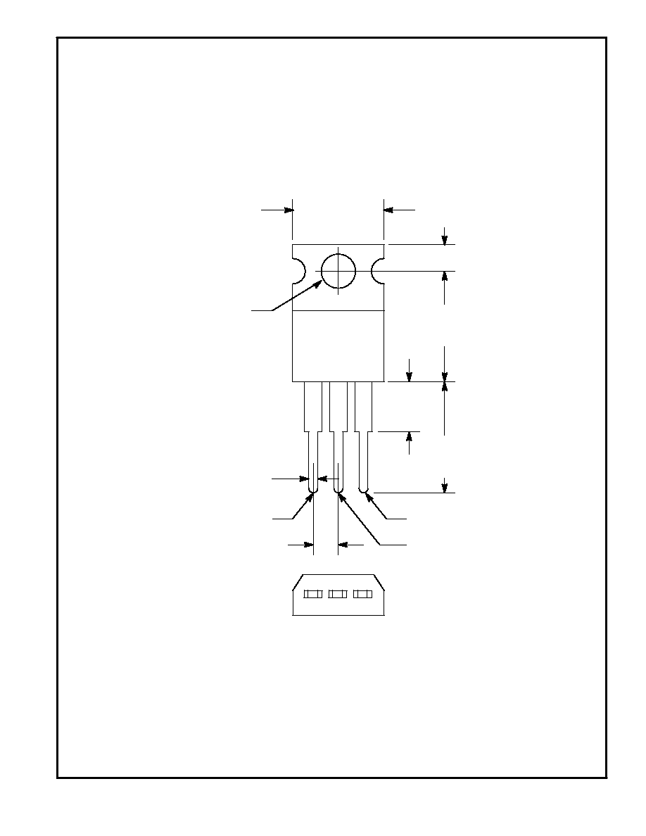
NTE2986
Logic Level MOSFET
N≠Channel, Enhancement Mode
High Speed Switch
Features:
D
Dynamic dv/dt Rating
D
Logic Level Gate Drive
D
R
DS
(on) Specified at V
GS
= 4V & 5V
D
+175
∞
C Operating Temperature
D
Fast Switching
D
Ease of Paralleling
D
Simple Drive Requirements
Absolute Maximum Ratings:
Drain Current, I
D
Continuous (V
GS
= 5V)
T
C
= +25
∞
C
50A
. . . . . . . . . . . . . . . . . . . . . . . . . . . . . . . . . . . . . . . . . . . . . . . . . . . . . . . . . . . . . . .
T
C
= +100
∞
C
36A
. . . . . . . . . . . . . . . . . . . . . . . . . . . . . . . . . . . . . . . . . . . . . . . . . . . . . . . . . . . . . .
Pulsed (Note 1)
200A
. . . . . . . . . . . . . . . . . . . . . . . . . . . . . . . . . . . . . . . . . . . . . . . . . . . . . . . . . . . . .
Total Power Dissipation (T
C
= +25
∞
C), P
D
150W
. . . . . . . . . . . . . . . . . . . . . . . . . . . . . . . . . . . . . . . . . . .
Derate Above 25
∞
C
1.0W/
∞
C
. . . . . . . . . . . . . . . . . . . . . . . . . . . . . . . . . . . . . . . . . . . . . . . . . . . . . . .
Gate≠Source Voltage, V
GS
±
10V
. . . . . . . . . . . . . . . . . . . . . . . . . . . . . . . . . . . . . . . . . . . . . . . . . . . . . . . . .
Single Pulsed Avalanche Energy (Note 2), E
AS
110mJ
. . . . . . . . . . . . . . . . . . . . . . . . . . . . . . . . . . . . . .
Peak Diode Recovery dv/dt (Note 3), dv/dt
4.5V/ns
. . . . . . . . . . . . . . . . . . . . . . . . . . . . . . . . . . . . . . . . .
Operating Junction Temperature Range, T
J
≠55
∞
to +175
∞
C
. . . . . . . . . . . . . . . . . . . . . . . . . . . . . . . . . .
Storage Temperature Range, T
stg
≠55
∞
to +175
∞
C
. . . . . . . . . . . . . . . . . . . . . . . . . . . . . . . . . . . . . . . . . .
Maximum Lead Temperature (During Soldering, 1.6mm from case, 10sec), T
L
+300
∞
C
. . . . . . . . . .
Mounting Torque, 6≠32 or M3 Screw
10 lbf
∑
in (1.1 N
∑
m)
. . . . . . . . . . . . . . . . . . . . . . . . . . . . . . . . . . . . .
Thermal Resistance:
Maximum Junction≠to≠Case, R
thJC
1.0K/W
. . . . . . . . . . . . . . . . . . . . . . . . . . . . . . . . . . . . . . . . . .
Typical Case≠to≠Sink (Mounting surface flat, smooth, and greased), R
thCS
0.5K/W
. . . . . . .
Maximum Junction≠to≠Ambient (Free Air Operation), R
thJA
62K/W
. . . . . . . . . . . . . . . . . . . . .
Note 1. Repetitive Rating: Pulse width limited by maximum junction temperature.
Note 2. L = 179
µ
H, V
DD
= 25V, R
G
= 25
, I
AS
= 51A, Starting T
J
= +175
∞
C.
Note 3. I
SD
51A, di/dt
250A/
µ
s, V
DD
V
(BR)DSS
, T
J
+175
∞
C.
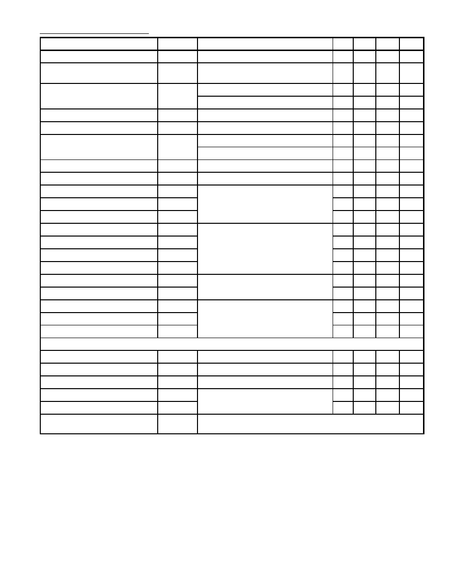
Electrical Characteristics: (T
C
= +25
∞
C unless otherwise specified)
Parameter
Symbol
Test Conditions
Min
Typ
Max
Unit
Drain≠Source Breakdown Voltage
BV
DSS
V
GS
= 0v, I
D
= 250
µ
A
60
≠
≠
V
Breakdown Voltage Temperature
Coefficient
V
(BR)DSS
/
T
J
Reference to +25
∞
C, I
D
= 1mA
≠
0.07
≠
V/
∞
C
Static Drain≠Source ON Resistance
R
DS(on)
V
GS
= 5V, I
D
= 31A, Note 4
≠
≠
0.028
V
GS
= 4V, I
D
= 25A, Note 4
≠
≠
0.039
Gate Threshold Voltage
V
GS(th)
V
DS
= V
GS
, I
D
= 250
µ
A
1.0
≠
2.0
V
Forward Transconductance
g
fs
V
DS
25V, I
D
= 31A, Note 4
23
≠
≠
mhos
Drain≠to≠Source Leakage Current
I
DSS
V
DS
= 60V, V
GS
= 0
≠
≠
25
µ
A
V
DS
= 48V, V
GS
= 0V, , T
C
= +150
∞
C
≠
≠
250
µ
A
Gate≠Source Leakage Forward
I
GSS
V
GS
= 10V
≠
≠
100
nA
Gate≠Source Leakage Reverse
I
GSS
V
GS
= ≠10V
≠
≠
≠100
nA
Total Gate Charge
Q
g
V
GS
= 5V, I
D
= 51A, V
DS
= 48V
≠
≠
66
nC
Gate≠Source Charge
Q
gs
≠
≠
12
nC
Gate≠Drain ("Miller") Charge
Q
gd
≠
≠
43
nC
Turn≠On Delay Time
t
d(on)
V
DD
= 30V
,
I
D
= 51A, R
G
= 4.6
,
≠
17
≠
ns
Rise Time
t
r
R
D
= 0.56
≠
230
≠
ns
Turn≠Off Delay Time
t
d(off)
≠
42
≠
ns
Fall Time
t
f
≠
110
≠
ns
Internal Drain Inductance
L
D
Between lead, 6mm (0.25") from
≠
4.5
≠
nH
Internal Source Inductance
L
S
package and center of die contact
≠
7.5
≠
nH
Input Capacitance
C
iss
V
GS
= 0V, V
DS
= 25V, f = 1MHz
≠
3300
≠
pF
Output Capacitance
C
oss
≠
1200
≠
pF
Reverse Transfer Capacitance
C
rss
≠
200
≠
pF
Source≠Drain Diode Ratings and Characteristics
Continuous Source Current
I
S
(Body Diode)
≠
≠
50
A
Pulse Source Current
I
SM
(Body Diode) Note 1
≠
≠
200
A
Diode Forward Voltage
V
SD
T
J
= +25
∞
C, I
S
= 51A, V
GS
= 0V, Note 4
≠
≠
2.5
V
Reverse Recovery Time
t
rr
T
J
= +25
∞
C, I
F
= 51A, di/dt = 100A/
µ
s,
≠
130
180
ns
Reverse Recovery Charge
Q
rr
Note 4
≠
0.84
1.3
µ
C
Forward Turn≠On Time
t
on
Intrinsic turn≠on time is neglegible
(turn≠on is dominated by L
S
+ L
D
)
Note 1. Repetitive Rating: Pulse width limited by maximum junction temperature.
Note 4. Pulse Test: Pulse Width
300
µ
s, Duty Cycle
2%.