
NTE3102
Photon Coupled Interrupter Module
NPN Transistor
Description:
The NTE3102 Interrupter Module is a gallium arsenide infrared emitting diode coupled to a silicon
phototransistor in a plastic housing. The packaging system is designed to optimize the mechanical
resolution, coupling efficiency, ambient light rejection, cost, and reliability. The gap in the housing pro-
vides a means of interrupting the signal with an opaque material, switching the output from an "ON"
into an "OFF" state.
Absolute Maximum Ratings: (T
A
= +25
∞
C unless otherwise specified)
Total Device
Operating Temperature Range, T
J
≠55
∞
to +100
∞
C
. . . . . . . . . . . . . . . . . . . . . . . . . . . . . . . . . . . . . . . . . .
Storage Temperature Range, T
stg
≠55
∞
to +100
∞
C
. . . . . . . . . . . . . . . . . . . . . . . . . . . . . . . . . . . . . . . . . .
Lead Temperature (During Soldering, 5sec Max), T
L
+260
∞
C
. . . . . . . . . . . . . . . . . . . . . . . . . . . . . . . . .
Infrared Emitting Diode
Forward Current, I
F
Continuous
60mA
. . . . . . . . . . . . . . . . . . . . . . . . . . . . . . . . . . . . . . . . . . . . . . . . . . . . . . . . . . . . . . . .
Peak (Pulse Width
1
µ
s, PRR
300pps)
3A
. . . . . . . . . . . . . . . . . . . . . . . . . . . . . . . . . . . . . . . .
Reverse Voltage, V
R
6V
. . . . . . . . . . . . . . . . . . . . . . . . . . . . . . . . . . . . . . . . . . . . . . . . . . . . . . . . . . . . . . . . .
Power Dissipation, P
E
100mW
. . . . . . . . . . . . . . . . . . . . . . . . . . . . . . . . . . . . . . . . . . . . . . . . . . . . . . . . . . .
Derate Above 25
∞
C
1.33mW/
∞
C
. . . . . . . . . . . . . . . . . . . . . . . . . . . . . . . . . . . . . . . . . . . . . . . . . . . .
Phototransistor
Power Dissipation, P
D
150mW
. . . . . . . . . . . . . . . . . . . . . . . . . . . . . . . . . . . . . . . . . . . . . . . . . . . . . . . . . . .
Derate Above 25
∞
C
2.0mW/
∞
C
. . . . . . . . . . . . . . . . . . . . . . . . . . . . . . . . . . . . . . . . . . . . . . . . . . . . .
Continuous Collector Current, I
C
100mA
. . . . . . . . . . . . . . . . . . . . . . . . . . . . . . . . . . . . . . . . . . . . . . . . . .
Collector≠Emitter Voltage, V
CEO
55V
. . . . . . . . . . . . . . . . . . . . . . . . . . . . . . . . . . . . . . . . . . . . . . . . . . . . . .
Emitter≠Collector Voltage, V
ECO
6V
. . . . . . . . . . . . . . . . . . . . . . . . . . . . . . . . . . . . . . . . . . . . . . . . . . . . . . .
Electrical Characteristics: (T
A
= +25
∞
C, Note 1 unless otherwise specified)
Parameter
Symbol
Test Conditions
Min
Typ
Max
Unit
Emitter
Reverse Breakdown Voltage
V
(BR)R
I
R
= 10
µ
A
6
≠
≠
V
Forward Voltage
V
F
I
F
= 60mA
≠
≠
1.7
V
Reverse Current
I
R
V
R
= 5V
≠
≠
100
nA
Capacitance
C
i
V = 0, f = 1MHz
≠
30
≠
pF
Note 1. Stray irradiation can alter values of characteristics. Adequate shielding should be provided.
Electrical Characteristics (Cont'd): (T
A
= +25
∞
C, Note 1 unless otherwise specified)
Parameter
Symbol
Test Conditions
Min
Typ
Max
Unit
Detector
Collector≠Emitter Breakdown Voltage
V
(BR)CEO
I
C
= 1mA
55
≠
≠
V
Emitter≠Collector Breakdown Voltage
V
(BR)ECO
I
E
= 100
µ
A
6
≠
≠
V
Collector Dark Current
I
CEO
V
CE
= 45V
≠
≠
100
nA
Capacitance
C
ce
V
CE
= 5V, f = 1MHz
≠
3.3
5.0
pF
Coupled
Photodiode Current
I
CE(on)
V
CE
= 5V, I
F
= 5mA
0.15
≠
≠
mA
V
CE
= 5V, I
F
= 20mA
1.0
≠
≠
mA
V
CE
= 5V, I
F
= 30mA
1.9
≠
≠
mA
Collector≠Emitter Saturation Voltage
V
CE(sat)
I
C
= 1.8mA, I
F
= 30mA
≠
≠
0.4
V
Turn≠On Time
t
on
V
CC
= 5V, I
F
= 30mA, R
L
= 2.5k
≠
8
≠
µ
s
Turn≠Off Time
t
off
≠
50
≠
µ
s
Note 1. Stray irradiation can alter values of characteristics. Adequate shielding should be provided.
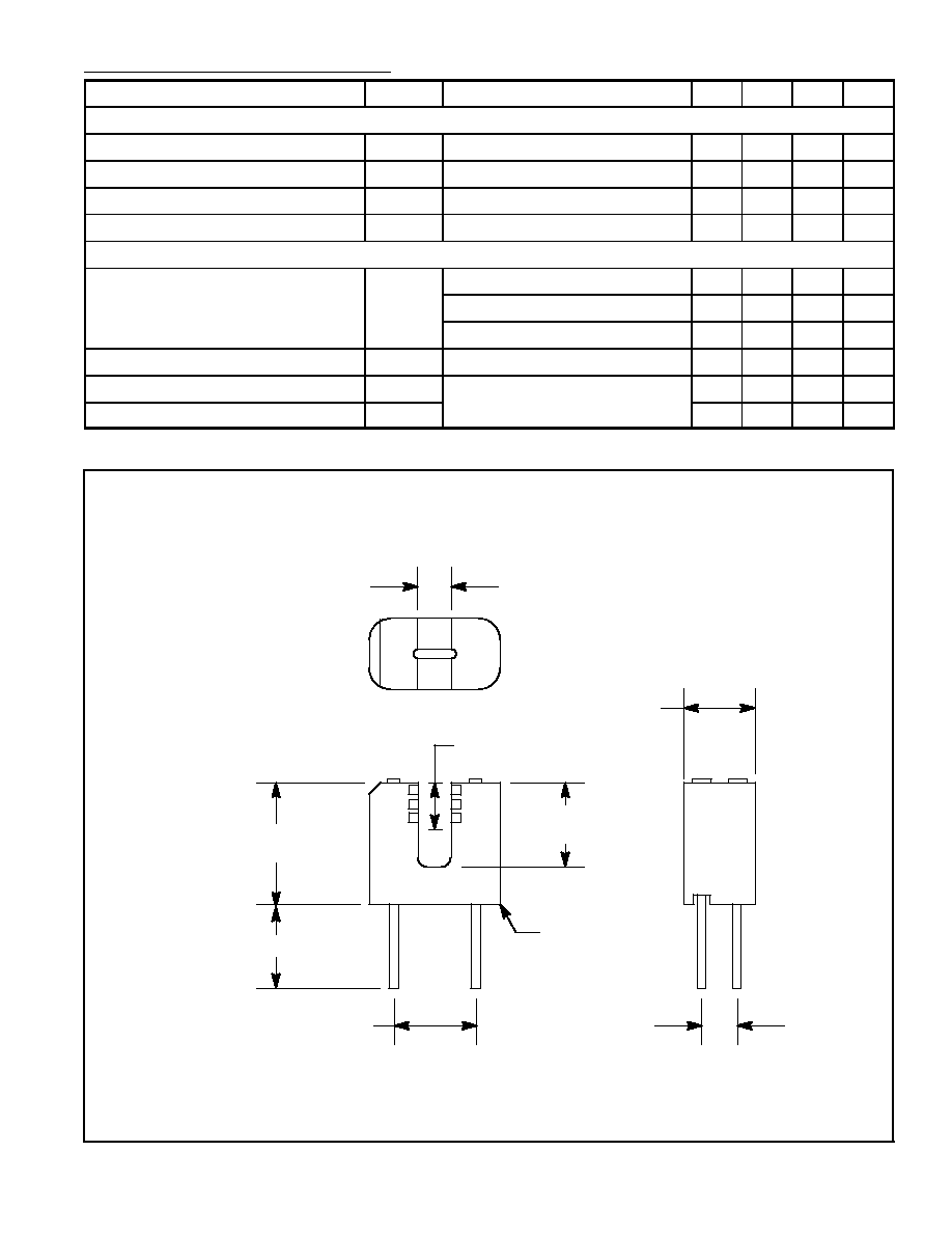
.303 (7.69)
Min
.124 (3.15
.110 (2.79) Max
.295 (7.49) Max
.246 (6.25)
Seating
Plane
.136 (3.54) Min
Sensing Area
.433 (11.0)
Max
.315 (8.0) Min
E
D
+
+
D ≠ Detector
E ≠ Emitter