NTE3097
Optoisolator
Zero Crossing TRIAC Driver
Description:
The NTE3097 is an optoisolator in a 6≠Lead DIP type package and contains a gallium arsenide IRED
optically coupled to a monolithic silicon detector performing the function of a Zero Voltage Crossing
bilateral TRIAC Driver. This device is designed for use with a TRIAC in the interface of logic systems
to equipment powered from 240VAC lines such as solid≠state relays, industrial controls, motors, sole-
noids, and consumer appliances, etc.
Features:
D
Simplifies Logic Control of 240VAC Power
D
Zero Voltage Crossing
D
High Breakdown Voltage: V
DRM
= 400V Min
D
High Isolation Voltage: V
ISO
= 7500V Guaranteed
D
Small, Economical 6≠Lead DIP Package
D
dv/dt of 2000V/
µ
s Typ., 1000V/
µ
s Guaranteed
Absolute Maximum Rating: (T
A
= +25
∞
C unless otherwise specified)
Infrared Emitting Diode
Reverse Voltage, V
R
6V
. . . . . . . . . . . . . . . . . . . . . . . . . . . . . . . . . . . . . . . . . . . . . . . . . . . . . . . . . . . . . . . . .
Continuous Forward Current, I
F
60mA
. . . . . . . . . . . . . . . . . . . . . . . . . . . . . . . . . . . . . . . . . . . . . . . . . . . .
Total Power Dissipation (T
A
= +25
∞
C, Negligible Power in Output Driver),P
D
120mW
. . . . . . . . . . . .
Derate Above 25
∞
C
1.41mW/
∞
C
. . . . . . . . . . . . . . . . . . . . . . . . . . . . . . . . . . . . . . . . . . . . . . . . . . . .
Output Driver
Off≠State Output Terminal Voltage, V
DRM
400V
. . . . . . . . . . . . . . . . . . . . . . . . . . . . . . . . . . . . . . . . . . . . .
Peak Repetitive Surge Current (PW = 100
µ
s, 120pps), I
TSM
1A
. . . . . . . . . . . . . . . . . . . . . . . . . . . . . .
Total Power Dissipation (T
A
= +25
∞
C),P
D
150mW
. . . . . . . . . . . . . . . . . . . . . . . . . . . . . . . . . . . . . . . . . . .
Derate Above 25
∞
C
1.76mW/
∞
C
. . . . . . . . . . . . . . . . . . . . . . . . . . . . . . . . . . . . . . . . . . . . . . . . . . . .
Total Device
Isolation Surge Voltage (Peak AC Voltage, 60Hz, 1sec Duration, Note 1), V
ISO
7500V
. . . . . . . . . . .
Total Power Dissipation (T
A
= +25
∞
C),P
D
250mW
. . . . . . . . . . . . . . . . . . . . . . . . . . . . . . . . . . . . . . . . . . .
Derate Above 25
∞
C
2.94mW/
∞
C
. . . . . . . . . . . . . . . . . . . . . . . . . . . . . . . . . . . . . . . . . . . . . . . . . . . .
Junction Temperature Range, T
J
≠40
∞
to +100
∞
C
. . . . . . . . . . . . . . . . . . . . . . . . . . . . . . . . . . . . . . . . . . .
Ambient Operating Temperature Range, T
A
≠40
∞
to +85
∞
C
. . . . . . . . . . . . . . . . . . . . . . . . . . . . . . . . . . .
Storage Temperature Range, T
stg
≠40
∞
to +150
∞
C
. . . . . . . . . . . . . . . . . . . . . . . . . . . . . . . . . . . . . . . . . .
Lead Temperature (During Soldering, 10sec), T
L
+260
∞
C
. . . . . . . . . . . . . . . . . . . . . . . . . . . . . . . . . . . .
Note 1. Isolation surge voltage is an internal dielectric breakdown rating. For this test, Pin1 and Pin2
are common, and Pin4, Pin5, and Pin6 are common.
Electrical Characteristics: (T
A
= +25
∞
C unless otherwise specified)
Parameter
Symbol
Test Conditions
Min
Typ
Max
Unit
Input LED
Reverse Leakage Current
I
R
V
R
= 6V
≠
0.05
10
µ
A
Forward Voltage
V
F
I
F
= 30mA
≠
1.3
1.5
V
Output Detector (I
F
= 0 unless otherwise specified)
Leakage With LED OFF
I
DRM1
Either Direction, V
DRM
= 400V, Note 2
≠
2
100
nA
Peak On≠State Voltage
V
TM
Either Direction, I
TM
= 100mA Peak
≠
1.8
3.0
V
Critical Rate of Rise of
Off≠State Voltage
dv/dt
Note 4
1000 2000
≠
V/
µ
s
Coupled
LED Trigger Current,
Current Required to
Latch Output
I
FT
Main Terminal Voltage = 3V, Note 3
≠
≠
15
mA
Holding Current
I
H
Either Direction
≠
100
≠
µ
A
Isolation Voltage
V
ISO
f = 60Hz, t = 1sec
7500
≠
≠
VAC(pk)
Zero Crossing
Inhibit Voltage
V
IH
I
F
= 15mA, MT1≠MT2 Voltage Above
Which Device Will Not Trigger
≠
5
20
V
Leakage in Inhibit State
I
DRM2
I
F
= 15mA, V
DRM
= 400V, Off≠State
≠
≠
500
µ
A
Note 2. Test voltage must be applied within dv/dt rating.
Note 3. This device is guaranteed to trigger at an I
F1
value less than or equal to max. I
FT
. Therefore,
recommended operating I
F
lies between max. I
FT
(15mA) and absolute max. I
F
(60mA).
Note 4. This is static dv/dt. Commutating dv/dt is a function of the load≠driving thyristor only.
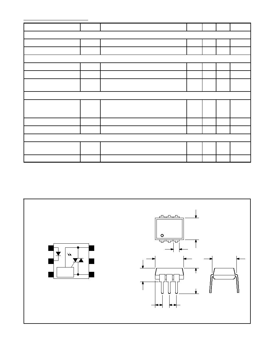
Pin Connection Diagram
.260
(6.6)
Max
.350
(8.89)
Max
.350 (8.89)
Max
.300 (7.62)
.200 (5.08)
Max
.085 (2.16)
Max
.070 (1.78)
Max
.100 (2.54)
1
2
3
5
4
6
Main Terminal
Substrate
Main Terminal
1
2
Anode
Cathode
3
N.C.
6
5
4
Do Not Connect
ZERO
CROSSING
CIRCUIT