NTE387
Silicon NPN Transistor
Power Amp, Switch
Features:
D
High Collector≠Emitter Sustaining Voltage
D
High DC Current Gain
D
Low Collector≠Emitter Saturation Voltage
D
Fast Switching Times
Absolute Maximum Ratings:
Collector≠Emitter Voltage, V
CEO
150V
. . . . . . . . . . . . . . . . . . . . . . . . . . . . . . . . . . . . . . . . . . . . . . . . . . . . .
Collector≠Base Voltage, V
CB
180V
. . . . . . . . . . . . . . . . . . . . . . . . . . . . . . . . . . . . . . . . . . . . . . . . . . . . . . .
Emitter≠Base Voltage, V
EB
6V
. . . . . . . . . . . . . . . . . . . . . . . . . . . . . . . . . . . . . . . . . . . . . . . . . . . . . . . . . . .
Collector Current, I
C
Continuous
50A
. . . . . . . . . . . . . . . . . . . . . . . . . . . . . . . . . . . . . . . . . . . . . . . . . . . . . . . . . . . . . . . . . .
Peak
100A
. . . . . . . . . . . . . . . . . . . . . . . . . . . . . . . . . . . . . . . . . . . . . . . . . . . . . . . . . . . . . . . . . . . . . .
Continuous Base Current, I
B
20A
. . . . . . . . . . . . . . . . . . . . . . . . . . . . . . . . . . . . . . . . . . . . . . . . . . . . . . . . .
Total Device Dissipation (T
C
= +25
∞
C), P
D
250W
. . . . . . . . . . . . . . . . . . . . . . . . . . . . . . . . . . . . . . . . . . .
Derate Above 25
∞
C
1.43W/
∞
C
. . . . . . . . . . . . . . . . . . . . . . . . . . . . . . . . . . . . . . . . . . . . . . . . . . . . . .
Operating Junction Temperature Range, T
J
≠65
∞
to +200
∞
C
. . . . . . . . . . . . . . . . . . . . . . . . . . . . . . . . . .
Storage Temperature Range, T
stg
≠65
∞
to +200
∞
C
. . . . . . . . . . . . . . . . . . . . . . . . . . . . . . . . . . . . . . . . . .
Thermal Resistance, Junction≠to≠Case, R
thJC
0.70
∞
C/W
. . . . . . . . . . . . . . . . . . . . . . . . . . . . . . . . . . . .
Note 1. Matched pairs are available upon request (NTE387MP). Matched pairs have their gain
specification (h
FE
) matched to within 10% of each other.
Electrical Characteristics: (T
C
= +25
∞
C unless otherwise specified)
Parameter
Symbol
Test Conditions
Min
Typ
Max
Unit
OFF Characteristics
Collector≠Emitter Sustaining Voltage
V
CEO(sus)
I
C
= 50mA, I
B
= 0, Note 2
150
≠
≠
V
Collector Cutoff Current
I
CEO
V
CE
= 75V, I
B
= 0
≠
≠
50
µ
A
I
CEX
V
CE
= 180V, V
EB(off)
= 1.5V
≠
≠
10
µ
A
V
CE
= 180V, V
EB(off)
= 1.5V, T
C
= +150
∞
C
≠
≠
1.0
µ
A
Emitter Cutoff Current
I
EBO
V
BE
= 6V, I
C
= 0
≠
≠
100
µ
A
Note 2. Pulse Test: Pulse Width
300
µ
s, Duty Cycle
2%.
Electrical Characteristics (Cont'd): (T
C
= +25
∞
C unless otherwise specified)
Parameter
Symbol
Test Conditions
Min
Typ
Max Unit
ON Characteristics (Note 2)
DC Current Gain
h
FE
V
CE
= 4V, I
C
= 1A
50
≠
≠
V
CE
= 4V, I
C
= 20A
30
≠
120
V
CE
= 4V, I
C
= 50A
10
≠
≠
Collector≠Emitter Saturation Voltage
V
CE(sat)
I
C
= 20A, I
B
= 2A
≠
≠
1
V
I
C
= 50A, I
B
= 10A
≠
≠
3
V
Base≠Emitter Saturation Voltage
V
BE(sat)
I
C
= 20A, I
B
= 2A
≠
≠
1.8
V
I
C
= 50A, I
B
= 10A
≠
≠
3.5
V
Base≠Emitter ON Voltage
V
BE(on)
V
CE
= 4V, I
C
= 20A
≠
≠
1.8
V
Dynamic Characteristics
Current Gain≠Bandwidth Product
f
T
V
CE
= 10V, I
C
= 1A, f
test
= 10MHz, Note 3
30
≠
≠
MHz
Output Capacitance
C
ob
V
CB
= 10V, I
E
= 0, f
test
= 0.1MHz
≠
≠
600
pF
Switching Characteristics
Rise Time
t
r
V
CC
= 80V, I
C
= 20A, I
B1
= 2A, V
BE(off)
= 5V
≠
≠
0.35
µ
s
Storage Time
t
s
V
CC
= 80V, I
C
= 20A, I
B1
= I
B2
= 2A
≠
≠
0.80
µ
s
Fall Time
t
f
≠
≠
0.25
µ
s
Note 2. Pulse Test: Pulse Width
300
µ
s, Duty Cycle
2%.
Note 3. f
T
= (h
fe
)
test
1.187
(30.16)
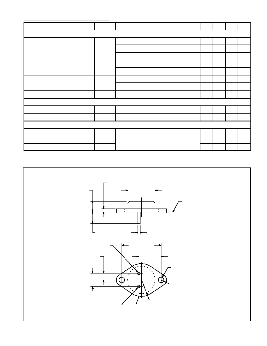
.875 (22.2)
Dia Max
.665
(16.9)
.430
(10.92)
Seating
Plane
.040 (1.02)
.312 (7.93) Min
.135 (3.45) Max
.350 (8.89)
Emitter
Collector/Case
Base
.215 (5.45)
.525 (13.35) R Max
.156 (3.96) Dia
(2 Holes)
.188 (4.8) R Max