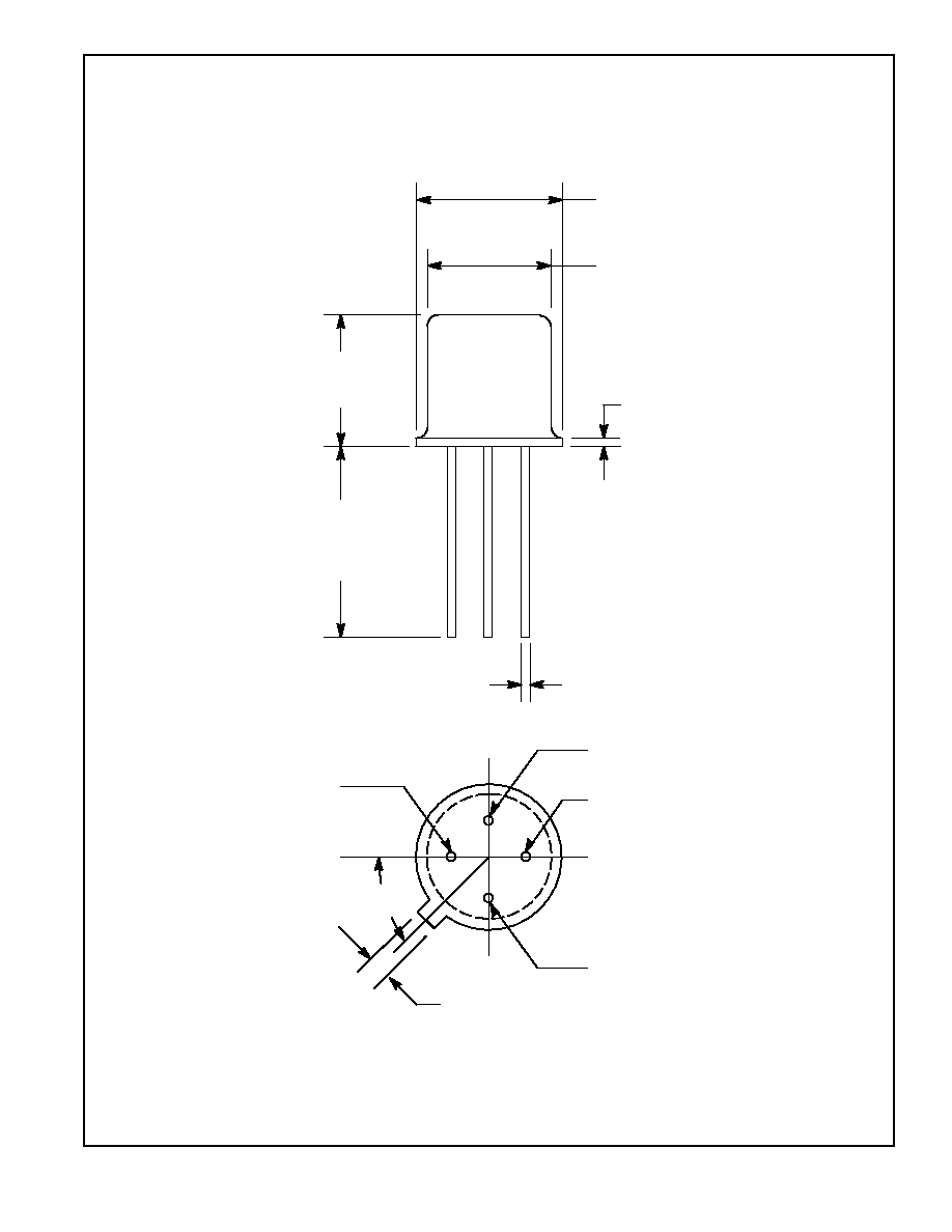
2
3
1
4
Gate 2
Gate 1
Source
Drain
NTE454
MOSFET, N≠Ch, Dual Gate,
TV UHF/RF Amp, Gate Protected
Description:
The NTE454 is a depletion mode dual gate MOSFET transistor designed for VHF amplifier and mixer
applications.
Features:
D
Low Reverse Transfer Capacitance ≠ C
rss
= 0.03pf (Max)
D
High Forward Transfer Admittance ≠ |y
fe
|
= 0≠20 mmhos
D
Diode Protected Gates
Absolute Maximum Ratings:
Drain Source Voltage, V
DSX
20Vdc
. . . . . . . . . . . . . . . . . . . . . . . . . . . . . . . . . . . . . . . . . . . . . . . . . . . . . . .
Drain≠Gate Voltage, V
DG1
30Vdc
. . . . . . . . . . . . . . . . . . . . . . . . . . . . . . . . . . . . . . . . . . . . . . . . . . . . . . . . .
V
DG2
30Vdc
. . . . . . . . . . . . . . . . . . . . . . . . . . . . . . . . . . . . . . . . . . . . . . . . . . . . . . . . .
Gate Current, I
G1
±
10mAdc
. . . . . . . . . . . . . . . . . . . . . . . . . . . . . . . . . . . . . . . . . . . . . . . . . . . . . . . . . . . . .
I
G2
±
10mAdc
. . . . . . . . . . . . . . . . . . . . . . . . . . . . . . . . . . . . . . . . . . . . . . . . . . . . . . . . . . . . .
Drain Current≠Continuous, I
D
60mAdc
. . . . . . . . . . . . . . . . . . . . . . . . . . . . . . . . . . . . . . . . . . . . . . . . . . . .
Total Power Dissipation (T
A
= +25
∞
C), P
D
360mW
. . . . . . . . . . . . . . . . . . . . . . . . . . . . . . . . . . . . . . . . . .
Derate above 25
∞
C
2.4mW/
∞
C
. . . . . . . . . . . . . . . . . . . . . . . . . . . . . . . . . . . . . . . . . . . . . . . . . . . . .
Total Power Dissipation (T
C
= +25
∞
C), P
D
1.2Watt
. . . . . . . . . . . . . . . . . . . . . . . . . . . . . . . . . . . . . . . . . .
Derate above 25
∞
C
8.0mW/
∞
C
. . . . . . . . . . . . . . . . . . . . . . . . . . . . . . . . . . . . . . . . . . . . . . . . . . . . .
Storage Channel Temperature Range, T
stg
≠65 to +200
∞
C
. . . . . . . . . . . . . . . . . . . . . . . . . . . . . . . . . .
Junction Temperature Range, T
J
≠65 to +175
∞
C
. . . . . . . . . . . . . . . . . . . . . . . . . . . . . . . . . . . . . . . . . . .
Lead Temperature, 1/16" from Seated Surface for 10 Seconds, T
L
300
∞
C
. . . . . . . . . . . . . . . . . . . . . .
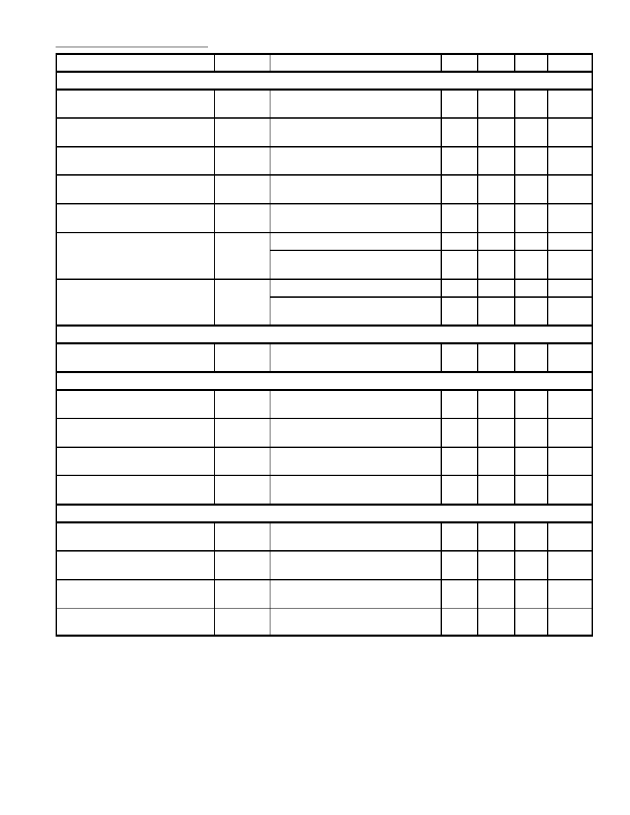
Electrical Characteristics: (T
A
= 25
∞
C unless otherwise noted)
Characteristics
Symbol
Test Conditions
Min
Typ
Max
Unit
OFF CHARACTERISTICS
Drain≠Source Breakdown
Voltage
V
(BR)DSX
I
D
= 10
µ
Adc, V
5
= 0,
V
GIS
= V
G25
= 5.0Vdc
20
≠
≠
Vdc
Gate 1= Source Breakdown
Voltage (Note 1)
V
(BR)G1SO
I
G1
=
±
10mAdc, V
GIS
= V
DS
= 0
±
6.0
±
12
±
30
Vdc
Gate 2≠Source Breakdown
Voltage (Note 1)
V
(BR)G2SO
I
G2
=
±
10mAdc, V
G15
= V
D5
= 0
±
5.0
±
12
±
30
Vdc
Gate 1 to Source Cutoff Voltage
V
GIS(off)
V
DS
= 15Vdc, V
G2S
= 4.0Vdc,
I
D
= 20
µ
Adc
≠0.5
≠1.5
≠5.0
Vdc
Gate 2 to Source Cutoff Voltage
V
G2S(off)
V
DS
= 15Vdc, V
G15
= 0,
I
D
= 20
µ
Adc
≠0.2
≠1.4
≠5.0
Vdc
Gate 1 Leakage Current
I
G1SS
V
GIS
=
±
5.0Vdc, V
G2S
= V
DS
= 0
≠
±
0.04
±
10
nAdc
V
G2S
= ≠5.0Vdc, V
G2S
= V
DS
= 0,
T
A
= 150
∞
C
≠
≠
≠10
µ
Adc
Gate 2 Leakage Current
I
G2SS
V
G2S
=
±
5.0Vdc, V
GIS
= V
DS
= 0
≠
±
0.05
±
10
nAdc
V
G2S
= ≠5.0Vdc, V
GIS
= V
DS
= 0,
T
A
= 150
∞
C
≠
≠
≠10
µ
Adc
ON CHARACTERISTICS
Zero≠Gate Voltage Drain
Current (Note 2)
I
DSS
V
DS
= 15Vdc, V
GIS
= 0,
V
G25
= 4.0Vdc
6.0
13
30
mAdc
SMALL≠SIGNAL CHARACTERISTICS
Forward Transfer Admittance
(Note 3)
|y
fe
|
V
DS
= 15Vdc, V
G2S
= 4.0Vdc,
V
GIS
= 0, f = 1.0kH
Z
8.0
12.8
20
mmhos
Input Capacitance
C
iss
V
DS
= 15Vdc, V
G2S
= 4.0Vdc,
I
D
= I
DSS
, f = 1.0MH
Z
≠
3.3
≠
pF
Output Capacitance
C
oss
V
DS
= 15Vdc, V
G2S
= 4.0Vdc,
I
D
= I
DSS
, f = 1.0MH
Z
≠
1.7
≠
pF
Reverse Transfer Capacitance
C
rss
V
DS
= 15Vdc, V
G2S
= 4.0Vdc,
I
D
= 10mAdc, f = 1.0MH
Z
0.005
0.014
0.03
pF
FUNCTIONAL CHARACTERISTICS
Noise Figure
NF
V
DD
= 18Vdc, V
GG
= 7.0Vdc,
f = 200MH
Z
≠
1.8
4.5
dB
Common Source Power Gain
G
ps
V
DD
= 18Vdc, V
GG
= 7.0Vdc,
f = 200MH
Z
15
20
25
dB
Bandwidth
BW
V
DD
= 18Vdc, V
GG
= 7.0Vdc,
f = 200MH
Z
5.0
≠
9.0
MH
Z
Gain Control Gate Supply
Voltage (Note 4)
V
GG(GC)
V
DD
= 18Vdc,
G
ps
= ≠30dB,
f = 200MH
Z
0
≠1.0
≠3.0
Vdc
Note 1. All gate breakdown voltages are measured while the device is conducting rated gate current. This ensures
that the gate≠voltage limiting network is functioning properly.
Note 2. Pulse Test: Pulse Width = 300
µ
s, Duty Cycle
2.0%
Note 3. This parameter must be measured with bias voltages supplied for less than 6 seconds to avoid overheating.
Note 4.
G
ps
is defined as the change in G
pe
from the values at V
GG
= 7.0V power gain conversion