
NTE56065
TRIAC, 600V
RM
, 12A,
High Commutation
Description:
The NTE56065 is a glass passivated, high commutation TRIAC in an isolated full≠pack type package
designed for use in circuits where high static and dynamic dV/dt and high dI/dt can occur. This device
will commutate the full rated RMS current at the maximum rated junction temperature, without the aid
of a snubber.
Absolute Maximum Ratings:
Repetitive Peak Off≠Sate Voltage (Note 1), V
DRM
600V
. . . . . . . . . . . . . . . . . . . . . . . . . . . . . . . . . . . . .
RMS On≠State Current (Full Sine Wave, T
HS
56
∞
C), I
T
(RMS)
12A
. . . . . . . . . . . . . . . . . . . . . . . . . .
Non≠Repetitive Peak On≠State Current, I
TSM
(Full Sine Wave, T
J
= +25
∞
C prior to Surge)
t = 20ms
95A
. . . . . . . . . . . . . . . . . . . . . . . . . . . . . . . . . . . . . . . . . . . . . . . . . . . . . . . . . . . . . . . . .
t = 16.7ms
105A
. . . . . . . . . . . . . . . . . . . . . . . . . . . . . . . . . . . . . . . . . . . . . . . . . . . . . . . . . . . . . . .
I
2
t for Fusing (t = 10ms), I
2
t
45A
2
sec
. . . . . . . . . . . . . . . . . . . . . . . . . . . . . . . . . . . . . . . . . . . . . . . . . . . . . .
Repetitive Rate≠of≠Rise of On≠State Current after Triggering, dI
T
/dt
(I
TM
= 20A, I
G
= 0.2A, dI
G
/dt = 0.2A/
µ
s)
100A/
µ
s
. . . . . . . . . . . . . . . . . . . . . . . . . . . . . . . . . . . . .
Peak Gate Current, I
GM
2A
. . . . . . . . . . . . . . . . . . . . . . . . . . . . . . . . . . . . . . . . . . . . . . . . . . . . . . . . . . . . . .
Peak Gate Voltage, V
GM
5V
. . . . . . . . . . . . . . . . . . . . . . . . . . . . . . . . . . . . . . . . . . . . . . . . . . . . . . . . . . . . .
Peak Gate Power, P
GM
5W
. . . . . . . . . . . . . . . . . . . . . . . . . . . . . . . . . . . . . . . . . . . . . . . . . . . . . . . . . . . . .
Average Gate Power (Over Any 20ms Period), P
G(AV)
500mW
. . . . . . . . . . . . . . . . . . . . . . . . . . . . . . . .
Operating Junction Temperature, T
J
+125
∞
C
. . . . . . . . . . . . . . . . . . . . . . . . . . . . . . . . . . . . . . . . . . . . . . .
Storage Temperature Range, T
stg
≠40
∞
to +150
∞
C
. . . . . . . . . . . . . . . . . . . . . . . . . . . . . . . . . . . . . . . . . .
Thermal Resistance, Junction≠to≠Heatsink (Full or Half Cycle), R
thJHS
With Heatsink Compound
4.0K/W
. . . . . . . . . . . . . . . . . . . . . . . . . . . . . . . . . . . . . . . . . . . . . . . . . .
Without Heatsink Compound
5.5K/W
. . . . . . . . . . . . . . . . . . . . . . . . . . . . . . . . . . . . . . . . . . . . . . .
Typical Thermal Resistance, Junction≠to≠Ambient, R
thJA
55K/W
. . . . . . . . . . . . . . . . . . . . . . . . . . . . .
Note 1. Although not recommended, off≠state voltages up to 800V may be applied without damage,
but the TRIAC may switch to the on≠state. The rate≠of≠rise of current should not exceed
15A/
µ
s.
Electrical Characteristics: (T
J
= +25
∞
C unless otherwise specfied)
Parameter
Symbol
Test Conditions
Min
Typ
Max
Unit
Static Characteristics
Gate Trigger Current
MT
2
(+), G (+)
I
GT
V
D
= 12V, I
T
= 0.1A, Note 2
2
18
50
mA
MT
2
(+), G (≠)
2
21
50
mA
MT
2
(≠), G (≠)
2
34
50
mA
Latching Current
MT
2
(+), G (+)
I
L
V
D
= 12V, I
T
= 0.1A
≠
31
60
mA
MT
2
(+), G (≠)
≠
34
90
mA
MT
2
(≠), G (≠)
≠
30
60
mA
Holding Current
I
H
V
D
= 12V, I
T
= 0.1A
≠
31
60
mA
On≠State Voltage
V
T
I
T
= 17A
≠
1.3
1.6
V
Gate Trigger Voltage
V
GT
V
D
= 12V, I
T
= 0.1A
≠
0.7
1.5
V
V
D
= 400V, I
T
= 0.1A, T
J
= +125
∞
C
0.25
0.4
≠
V
Off≠State Leakage Current
I
D
V
D
= 600V, T
J
= +125
∞
C
≠
0.1
0.5
mA
Dynamic Characteristics
Critical Rate≠of≠Rise of
Off≠State Voltage
dV
D
/dt
V
DM
= 402V, T
J
= +125
∞
C,
Exponential Waveform, Gate Open
1000
4000
≠
V/
µ
s
Critical Rate≠of≠Change of
Commutating Current
dI
com
/dt
V
DM
= 400V, T
J
= +125
∞
C, I
T
RMS = 12A,
without Snubber, Gate Open
≠
24
≠
A/ms
Gate Controlled Turn≠On Time
t
gt
I
TM
= 12A, V
D
= V
DRM
max, I
G
= 0.1A,
dI
G
/dt = 5A/
µ
s
≠
2
≠
µ
s
Isolation Characteristics
RMS Isolation Voltage from All
3 Pins to External Heatsink
V
ISOL
f = 50 ≠ 60Hz, Sinusoidal Waveform,
R.H.
65%, Clean and Dustfree
≠
≠
2500
V
Capacitance from T2 to
External Heatsink
C
ISOL
f = 1MHz
≠
10
≠
pF
Note 2. Device does not trigger in the MT
2
(≠), G (+) quadrant.
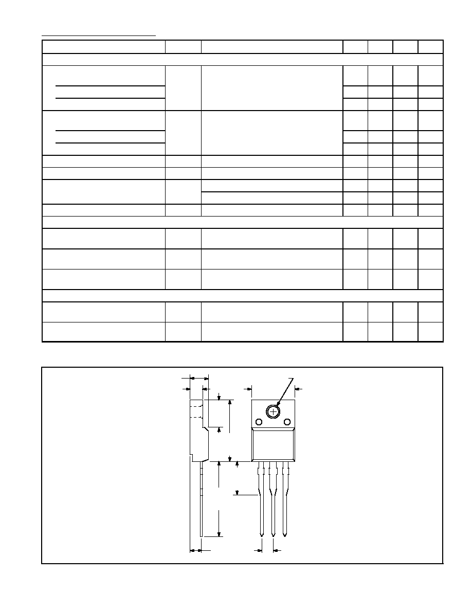
.126 (3.2) Dia Max
.181 (4.6) Max
.405 (10.3)
Max
.114 (2.9)
.622
(15.0)
Max
.252
(6.4)
.118
(3.0)
Max
MT
1
MT
2
G
Isol
.100 (2.54)
.098 (2.5)
.531
(13.5)
Min