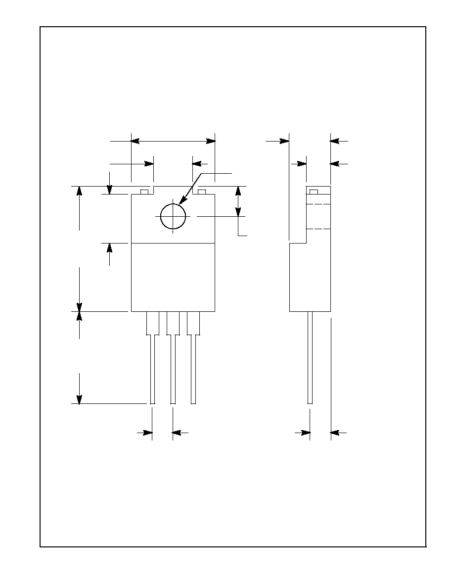
NTE5440
Silicon Controlled Rectifier (SCR)
800V, 10A, Isolated Tab
Applications:
D
Temperature Control
D
Motor Control
D
Transformerless Power Supply Regulators
D
Relay and Coil Pulsing
D
Power Supply Crowbar Protection
Absolute Maximum Ratings:
Anode to Cathode
Non≠Repetitive Peak Voltages (t
10ms, Note 1), V
DSM
, V
RSM
800V
. . . . . . . . . . . . . . . . . . . . . .
Repetitive Peak Voltages (
0.01), V
DRM
, V
RRM
800V
. . . . . . . . . . . . . . . . . . . . . . . . . . . . . . . . . . .
Peak Working Voltages, V
DWM
, V
RWM
400V
. . . . . . . . . . . . . . . . . . . . . . . . . . . . . . . . . . . . . . . . . . . .
Continuous Voltages, V
D
, V
R
400V
. . . . . . . . . . . . . . . . . . . . . . . . . . . . . . . . . . . . . . . . . . . . . . . . . . . .
Average On≠State Current, I
T(AV)
(Averaged over any 20ms period) up to T
h
= +74
∞
C
5.7A
. . . . . . . . . . . . . . . . . . . . . . . . . . .
RMS On≠State Current, I
T(RMS)
9A
. . . . . . . . . . . . . . . . . . . . . . . . . . . . . . . . . . . . . . . . . . . . . . . . . . . .
Repetitive Peak On≠State Current, I
TRM
65A
. . . . . . . . . . . . . . . . . . . . . . . . . . . . . . . . . . . . . . . . . . . .
Non≠Repetitive Peak On≠State Current, I
TSM
(t = 10ms, Half≠Sinewave, T
J
= +110
∞
C prior to surge, with Reapplied V
RWMmax
)
100A
.
I
2
t for Fusing (t = 10ms), I
2
t
50A
2
s
. . . . . . . . . . . . . . . . . . . . . . . . . . . . . . . . . . . . . . . . . . . . . . . . . . . . .
Rate of Rise of On≠State Current after Triggering, dI
T
/dt
(I
G
= 50mA to I
T
= 20A, dI
G
/dt = 50mA/
µ
s)
50A/
µ
s
. . . . . . . . . . . . . . . . . . . . . . . . . . . . . . . . .
Gate to Cathode
Reverse Peak Voltage, V
RGM
5V
. . . . . . . . . . . . . . . . . . . . . . . . . . . . . . . . . . . . . . . . . . . . . . . . . . . . . .
Average Power Dissipation (Averaged over any 20ms period), P
G(AV)
500mW
. . . . . . . . . . . . . . .
Peak Power Dissipation, P
GM
5W
. . . . . . . . . . . . . . . . . . . . . . . . . . . . . . . . . . . . . . . . . . . . . . . . . . . . .
Temperatures
Operating Junction Temperature, T
J
+110
∞
C
. . . . . . . . . . . . . . . . . . . . . . . . . . . . . . . . . . . . . . . . . . . .
Storage Temperature Range, T
stg
≠40
∞
to +125
∞
C
. . . . . . . . . . . . . . . . . . . . . . . . . . . . . . . . . . . . . . .
Maximum Lead Temperature (During Soldering, less than 5sec)
+275
∞
C
. . . . . . . . . . . . . . . . . . . .
Note 1. Although not recommended, higher Off≠State voltages may be applied without damage, but
the thyristor may switch into the On≠State. The Rate≠of≠Rise of On≠State current should
not exceed 15A/
µ
s.
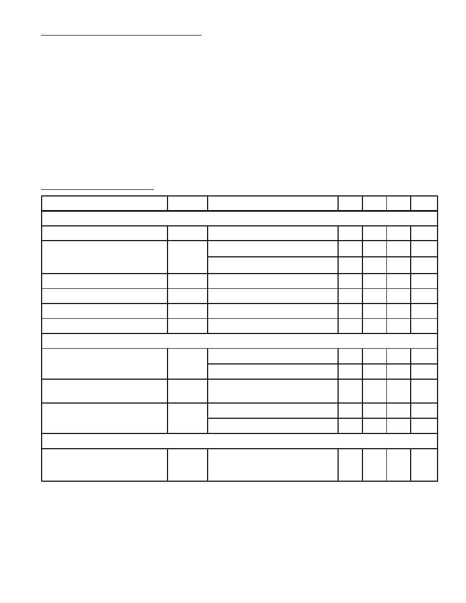
Absolute Maximum Ratings (Cont'd):
Isolation:
Minimum From all Three Pins to External Heatsink (Peak), V
isol
1000V
. . . . . . . . . . . . . . . . . . . . .
Typical Capacitance from Anode to External Heatsink, C
isol
12pf
. . . . . . . . . . . . . . . . . . . . . . . . . . .
Thermal Characteristics:
Thermal Resistance from Junction to External Heatsink, R
thj≠h
With Heatsink Compound
4.5K/W
. . . . . . . . . . . . . . . . . . . . . . . . . . . . . . . . . . . . . . . . . . . . . . .
Without Heatsink Compound
6.5K/W
. . . . . . . . . . . . . . . . . . . . . . . . . . . . . . . . . . . . . . . . . . . .
Thermal Resistance from Junction≠to≠Ambient in Free Air, R
thJA
(Mounted on a printed circuit board at a = any lead length
and with copper laminate, Note 2)
55K/W
. . . . . . . . . . . . . . . . . . . . . . . . . . . . . . . . . . . . . . . .
Note 2. The quoted values of R
thJA
should be used only when no leads of other dissipating compo-
nents run to the same tie≠point.
Electrical Characteristics: (T
J
= +110
∞
C unless otherwise specified)
Parameter
Symbol
Test Conditions
Min
Typ
Max
Unit
Anode to Cathode
On≠State Voltage
V
T
I
T
= 23A, T
J
= 25
∞
C, Note 3
≠
≠
1.75
V
Rate of Rise of Off≠State
dV
D
/dt
R
GK
= Open Circuit
≠
≠
50
V/
µ
s
Voltage that will not
Trigger any Device
R
GK
= 100
≠
≠
200
V/
µ
s
Reverse Current
I
R
V
R
= 400V
≠
≠
0.5
mA
Off≠State Current
I
D
V
D
= 400V
≠
≠
0.5
mA
Latching Current
I
L
T
J
= 25
∞
C
≠
≠
40
mA
Holding Current
I
H
T
J
= 25
∞
C
≠
≠
20
mA
Gate to Cathode
Gate≠Trigger Voltage
V
GT
V
D
= 6V, T
J
= 25
∞
C
1.5
≠
≠
V
V
D
= 6V, T
J
= ≠40
∞
C
2.3
≠
≠
V
Voltage that will not
Trigger any Device
V
GD
V
D
= 800V
≠
≠
250
mV
Gate≠Trigger Current
I
GT
V
D
= 6V, T
J
= 25
∞
C
15
≠
≠
mA
V
D
= 6V, T
J
= ≠40
∞
C
20
≠
≠
mA
Switching Characteristice
Gate≠Controlled Turn≠On Time
(t
gt
= t
d
+ t
r
) when Switched
from V
D
= 800V to I
T
= 40A
t
gt
I
GT
= 100mA, dI
g
/dt = 5A/
µ
s,
T
J
= 25
∞
C
≠
2
≠
µ
s
Note 3. Measured under pulse conditions to avoid excessive dissipation.