NTE5480 thru NTE5487
Silicon Controlled Rectifier (SCR)
8 Amp
Description:
The NTE5480 through NTE5487 are multi≠purpose PNPN silicon controlled rectifiers in a TO64 type
package suited for industrial and consumer applications. These 8 amp devices are available in volt-
ages ranging from 25V to 600V.
Features:
D
Uniform Low≠Level Noise≠Immune Gate Triggering: I
GT
= 10mA Typ @ T
C
= +25
∞
C
D
Low Forward "ON" Voltage: v
T
= 1V Typ @ 5A @ +25
∞
C
D
High Surge≠Current Capability: I
TSM
= 100A Peak
D
Shorted Emitter Construction
Absolute Maximum Ratings: (T
J
= ≠40
∞
to +100
∞
C unless otherwise specified)
Peak Repetitive Forward and Reverse Blocking Voltage (Note 1), V
DRM
or V
RRM
NTE5480
25V
. . . . . . . . . . . . . . . . . . . . . . . . . . . . . . . . . . . . . . . . . . . . . . . . . . . . . . . . . . . . . . . . . . . .
NTE5481
50V
. . . . . . . . . . . . . . . . . . . . . . . . . . . . . . . . . . . . . . . . . . . . . . . . . . . . . . . . . . . . . . . . . . . .
NTE5482
100V
. . . . . . . . . . . . . . . . . . . . . . . . . . . . . . . . . . . . . . . . . . . . . . . . . . . . . . . . . . . . . . . . . . .
NTE5483
200V
. . . . . . . . . . . . . . . . . . . . . . . . . . . . . . . . . . . . . . . . . . . . . . . . . . . . . . . . . . . . . . . . . . .
NTE5484
300V
. . . . . . . . . . . . . . . . . . . . . . . . . . . . . . . . . . . . . . . . . . . . . . . . . . . . . . . . . . . . . . . . . . .
NTE5485
400V
. . . . . . . . . . . . . . . . . . . . . . . . . . . . . . . . . . . . . . . . . . . . . . . . . . . . . . . . . . . . . . . . . . .
NTE5486
500V
. . . . . . . . . . . . . . . . . . . . . . . . . . . . . . . . . . . . . . . . . . . . . . . . . . . . . . . . . . . . . . . . . . .
NTE5487 (This device is discontinued)
600V
. . . . . . . . . . . . . . . . . . . . . . . . . . . . . . . . . . . . . .
Forward Current RMS, I
T(RMS)
8A
. . . . . . . . . . . . . . . . . . . . . . . . . . . . . . . . . . . . . . . . . . . . . . . . . . . . . . . .
Peak Forward Surge Current (One Cycle, 60Hz, T
J
= ≠40
∞
to +100
∞
C, I
TSM
100A
. . . . . . . . . . . . . . .
Circuit Fusing (t
8.3ms, T
J
= ≠40
∞
to +100
∞
C), I
2
t
40A
2
s
. . . . . . . . . . . . . . . . . . . . . . . . . . . . . . . . . . .
Peak Gate Power, P
GM
5W
. . . . . . . . . . . . . . . . . . . . . . . . . . . . . . . . . . . . . . . . . . . . . . . . . . . . . . . . . . . . .
Average Gate Power, P
G(AV)
0.5W
. . . . . . . . . . . . . . . . . . . . . . . . . . . . . . . . . . . . . . . . . . . . . . . . . . . . . . . .
Peak Gate Current, I
GM
2A
. . . . . . . . . . . . . . . . . . . . . . . . . . . . . . . . . . . . . . . . . . . . . . . . . . . . . . . . . . . . . .
Peak Gate Voltage (Note 2), V
GM
10V
. . . . . . . . . . . . . . . . . . . . . . . . . . . . . . . . . . . . . . . . . . . . . . . . . . . .
Operating Temperature Range, T
J
≠40
∞
to +100
∞
C
. . . . . . . . . . . . . . . . . . . . . . . . . . . . . . . . . . . . . . . . . .
Storage Temperature Range, T
stg
≠40
∞
to +150
∞
C
. . . . . . . . . . . . . . . . . . . . . . . . . . . . . . . . . . . . . . . . . .
Typical Thermal Resistance, Junction≠to≠Case, R
thJC
1.5
∞
C/W
. . . . . . . . . . . . . . . . . . . . . . . . . . . . . .
Typical Thermal Resistance, Case≠to≠Ambient, R
thJA
50
∞
C/W
. . . . . . . . . . . . . . . . . . . . . . . . . . . . . . . .
Note 1. Ratings apply for zero or negative gate voltage. Devices should not be tested for blocking
capability in a manner such that the voltage applied exceeds the rated blocking voltage.
Note 2. Devices should not be operated with a positive bias applied to the gate concurrently with a
negative potential applied to the anode.
Electrical Characteristics: (T
C
= +25
∞
C unless otherwise specified)
Parameter
Symbol
Test Conditions
Min
Typ
Max
Unit
Peak Forward or Reverse
I
DRM
,
Rated V
DRM
or V
RRM
, T
J
= +25
∞
C
≠
≠
10
µ
A
Blocking Current
I
RRM
Gate Open
T
J
= +100
∞
C
≠
≠
2
mA
Gate Trigger Current (Continuous DC)
I
GT
V
D
= 7V, R
L
= 100
,
≠
10
30
mA
Note 3
T
C
= ≠40
∞
C
≠
≠
60
mA
Gate Trigger Voltage (Continuous DC)
V
GT
V
D
= 7V, R
L
= 100
≠
0.75
1.5
V
T
C
= ≠40
∞
C
≠
≠
2.5
V
T
J
= +100
∞
C
0.2
≠
≠
V
Forward "ON" Voltage
v
TM
I
TM
= 15.7A, Note 4
≠
1.4
2.0
V
Holding Current
I
H
V
D
= 7V, Gate Open
≠
10
30
mA
T
C
= ≠40
∞
C
≠
≠
60
mA
Turn≠On Time (t
d
+ t
r
)
t
on
I
G
= 20mA, I
F
= 5A, V
D
= Rated V
DRM
≠
1
≠
µ
s
Turn≠Off Time
t
off
I
F
= 5A, I
R
= 5A,
≠
15
≠
µ
s
dv/dt = 30V/
µ
s
T
J
= +100
∞
C,
V
D
= Rated V
DRM
≠
25
≠
µ
s
Forward Voltage Application Rate
(Exponential)
dv/dt
Gate Open, T
J
= +100
∞
C,
V
D
= Rated V
DRM
≠
50
≠
V/
µ
s
Note 3. For optimum operation, i.e. faster turn≠on, lower switching losses, best di/dt capability, rec-
ommended I
GT
= 200mA minimum.
Note 4. Pulsed, 1ms max., Duty Cycle
1%.
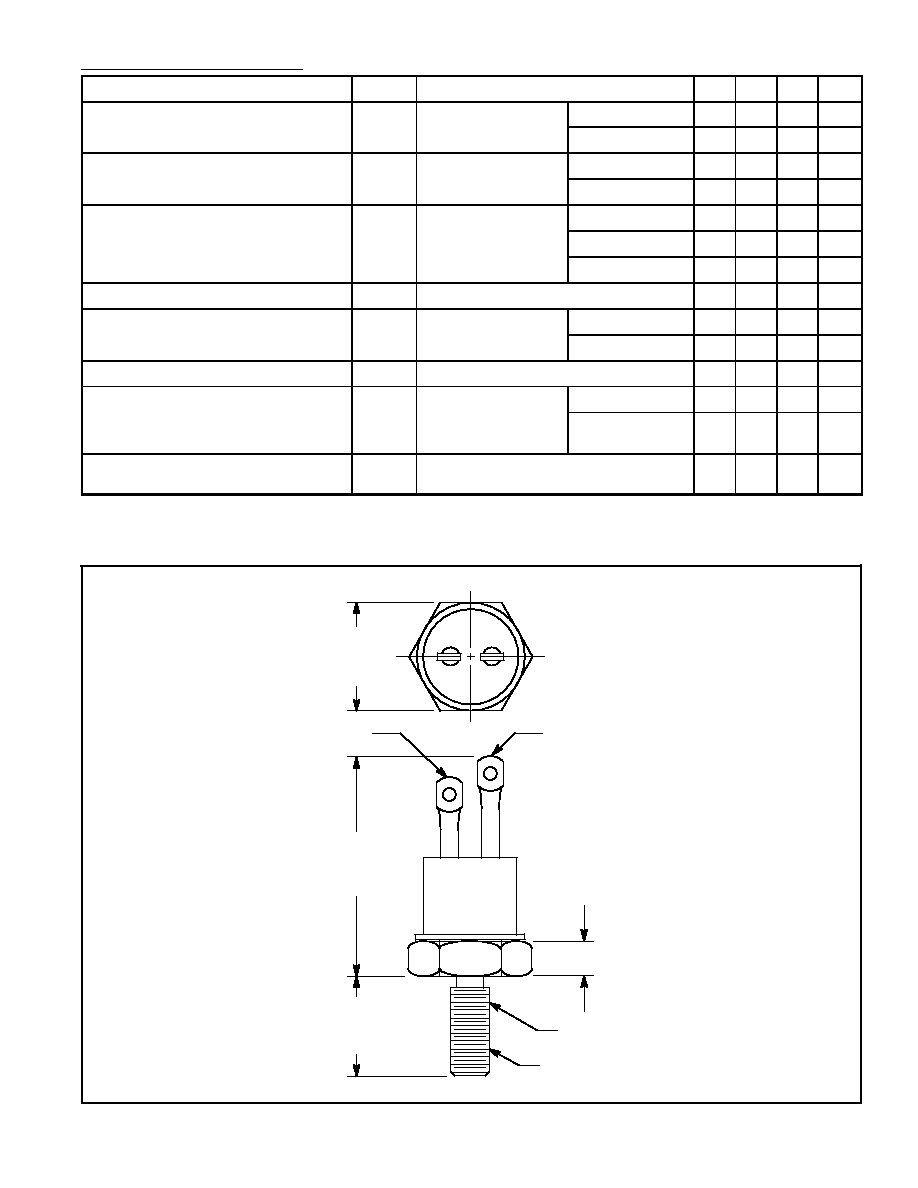
.125 (3.17) Max
.431
(10.98
Max
.855
(21.7)
Max
.453
(111.5)
Max
10≠32 UNF≠2A
Anode
Cathode
Gate