
NTE56019 and NTE56020
TRIAC, 25 Amp
Description:
The NTE56019 and NTE56020 are 25 Amp TRIACs with a repetitive peak blocking of 200V and
400V respectively. These devices may be gate triggered from a blocking to conduction state for
either polarity of applied voltage and are designed for AC switching and phase control applications
such as speed and temperature modulation controls, lighting controls, and static switching relays.
The triggering signal is normally applied between the Gate and MT
1
.
Features:
D
Electrically Isolated TO220 Type Package
D
Glass≠Passivated Junctions
D
Surge Capability: Up to 400A
Absolute Maximum Ratings: (T
A
= +25
∞
C, 60Hz, with a resistive load unless otherwise specified)
Repetitive Peak Blocking Voltage (Note 1), V
DRM
NTE56019
200V
. . . . . . . . . . . . . . . . . . . . . . . . . . . . . . . . . . . . . . . . . . . . . . . . . . . . . . . . . . . . . . . . .
NTE56020
400V
. . . . . . . . . . . . . . . . . . . . . . . . . . . . . . . . . . . . . . . . . . . . . . . . . . . . . . . . . . . . . . . . .
RMS On≠State Current (Conduction Angle of 360
∞
, T
C
= ≠40
∞
to +125
∞
C), I
T(RMS)
25A
. . . . . . . . . .
Non≠Repetitive On≠State Current (One Cycle), I
TSM
60Hz
250A
. . . . . . . . . . . . . . . . . . . . . . . . . . . . . . . . . . . . . . . . . . . . . . . . . . . . . . . . . . . . . . . . . . . . . .
50Hz
208A
. . . . . . . . . . . . . . . . . . . . . . . . . . . . . . . . . . . . . . . . . . . . . . . . . . . . . . . . . . . . . . . . . . . . . .
Fusing Current (t = 8.3ms), I
2
t
259A
2
s
. . . . . . . . . . . . . . . . . . . . . . . . . . . . . . . . . . . . . . . . . . . . . . . . . . . .
Peak Gate Current (Pulse Width
10
µ
s Max), I
GM
2A
. . . . . . . . . . . . . . . . . . . . . . . . . . . . . . . . . . . . . . .
Peak Gate Dissipation (Pulse Width
10
µ
s, I
GT
I
GTM
), P
GM
20W
. . . . . . . . . . . . . . . . . . . . . . . . . . .
Gate Dissipation, P
G(AV)
500mW
. . . . . . . . . . . . . . . . . . . . . . . . . . . . . . . . . . . . . . . . . . . . . . . . . . . . . . . . . .
Operating Junction Temperature Range, T
J
≠40
∞
to +125
∞
C
. . . . . . . . . . . . . . . . . . . . . . . . . . . . . . . . . .
Storage Temperature Range, T
stg
≠40
∞
to +125
∞
C
. . . . . . . . . . . . . . . . . . . . . . . . . . . . . . . . . . . . . . . . . .
Thermal Resistance, Junction≠to≠Case, R
thJC
1.5K/W
. . . . . . . . . . . . . . . . . . . . . . . . . . . . . . . . . . . . . .
Thermal Resistance, Junction≠to≠Ambient, R
thJA
60K/W
. . . . . . . . . . . . . . . . . . . . . . . . . . . . . . . . . . . .
Lead Temperature (During Soldering, 1/16" from case, 10sec max), T
L
+230
∞
C
. . . . . . . . . . . . . . . . .
Note 1. For either polarity of MT
2
with reference to MT
1
terminal.
Electrical Characteristics: (T
A
= +25
∞
C unless otherwise specified)
Parameter
Symbol
Test Conditions
Min
Typ
Max
Unit
Off≠State Leakage Current
I
DRM
V
D
= V
DRM
, T
J
= +25
∞
C, Note 1
≠
≠
0.1
mA
V
D
= V
DRM
, T
J
= +125
∞
C, Note 1
≠
≠
3
mA
On≠State Voltage
V
TM
I
T(RMS)
= 25A, Note 1
≠
≠
1.8
V
Note 1. For either polarity of MT
2
with reference to MT
1
terminal.
Electrical Characteristics (Cont'd): (T
A
= +25
∞
C unless otherwise specified)
Parameter
Symbol
Test Conditions
Min
Typ
Max
Unit
Gate Trigger Current
I
GT
V
D
= 12V, T
C
= ≠40
∞
to +125
∞
C
≠
≠
80
mA
Gate Trigger Voltage
V
GT
V
D
= 12V, Quadrants I, II, and III, Note 2
≠
≠
2.5
V
Holding Current
I
H
Gate Open, Note 1, Note 3
≠
≠
100
mA
Gate Controlled Turn≠On Time
t
gt
I
GT
= 500mA, 0.1
µ
s Rise Time
≠
4
≠
µ
s
Critical Rate≠of≠Rise
dv/dt
V
D
= V
DRM
, Gate Open, T
C
= +125
∞
C, Note 1
250
≠
≠
V/
µ
s
Critical Rate≠of≠Rise, Off≠State
dv/dt
c
V
D
= V
DRM
, I
T
= 25A, di/dt = 13.5A/ms,
Gate Unenergized, Note 1
5
≠
≠
V/
µ
s
Note 1. For either polarity of MT
2
with reference to MT
1
terminal.
Note 2. For either polarity of gate voltage with reference to electrode MT
1
.
Note 3. Initial On≠State Current = 400mA (DC).
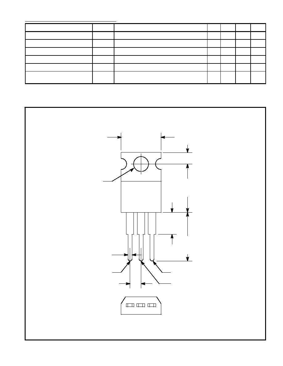
.250 (6.35)
Max
.500
(12.7)
Max
.500
(12.7)
Min
.110 (2.79)
.420 (10.67)
Max
.070 (1.78) Max
MT
1
.100 (2.54)
MT
2
Gate
.147 (3.75)
Dia Max
Isolated