
NTE5661
TRIAC, 10 Amp
Description:
The NTE5661 is a TRIAC in a TO64 type stud mount package designed primarily for full≠wave AC
control applications such as light dimmers, motor controls, heating controls, power supplies or wher-
ever full≠wave silicon gate controlled solid≠state devices are needed. TRIAC type thyristors switch
from a blocking to a conducting state for either polarity of applied anode voltage with positive or nega-
tive gate triggering.
Features:
D
Low "ON" Voltage
D
Gate Triggering Guaranteed in Four Modes
Absolute Maximum Ratings:
Repetitive Peak Off≠State Voltage (T
J
= +100
∞
C, Note 1), V
DRM
50V
. . . . . . . . . . . . . . . . . . . . . . . . . .
On≠State RMS Current (T
C
= +75
∞
C), I
T
RMS
10A
. . . . . . . . . . . . . . . . . . . . . . . . . . . . . . . . . . . . . . . . . .
Peak Surge Current (One Full Cycle, 60Hz, T
J
= ≠40
∞
to +100
∞
C), I
TSM
100A
. . . . . . . . . . . . . . . . . .
Circuit Fusing Considerations (T
J
= ≠40
∞
to +100
∞
C, t = 1.0 to 8.3ms), I
2
t
40A
2
sec
. . . . . . . . . . . . . .
Peak Gate Power, P
GM
10W
. . . . . . . . . . . . . . . . . . . . . . . . . . . . . . . . . . . . . . . . . . . . . . . . . . . . . . . . . . . .
Average Gate Power, P
G(AV)
0.5W
. . . . . . . . . . . . . . . . . . . . . . . . . . . . . . . . . . . . . . . . . . . . . . . . . . . . . . . .
Peak Gate Current, I
GM
2A
. . . . . . . . . . . . . . . . . . . . . . . . . . . . . . . . . . . . . . . . . . . . . . . . . . . . . . . . . . . . . .
Operating Junction Temperature Range, T
J
≠40
∞
to +100
∞
C
. . . . . . . . . . . . . . . . . . . . . . . . . . . . . . . . . .
Storage Temperature Range, T
stg
≠40
∞
to +150
∞
C
. . . . . . . . . . . . . . . . . . . . . . . . . . . . . . . . . . . . . . . . . .
Thermal Resistance, Junction≠to≠Case, R
thJC
2
∞
C/W
. . . . . . . . . . . . . . . . . . . . . . . . . . . . . . . . . . . . . . .
Thermal Resistance, Junction≠to≠Ambient, R
thJA
50
∞
C/W
. . . . . . . . . . . . . . . . . . . . . . . . . . . . . . . . . . . .
Stud Torque
15 in. lb.
. . . . . . . . . . . . . . . . . . . . . . . . . . . . . . . . . . . . . . . . . . . . . . . . . . . . . . . . . . . . . . . . . . .
Note 1. Ratings apply for open gate conditions. Thyristor devices shall not be tested with a constant
current source for blocking capability such that the voltage applied exceeds the rated block-
ing voltage.
Electrical Characteristics: (T
C
= +25
∞
C unless otherwise specified)
Parameter
Symbol
Test Conditions
Min
Typ
Max Unit
Peak Blocking Current (Either Direction)
I
DRM
V
DRM
= 50V, T
J
= +100
∞
C, Gate Open
≠
≠
2.0
mA
On≠State Voltage (Either Direction)
V
TM
I
TM
= 14A Peak
≠
1.3
1.8
V
Gate Trigger Current, Continuous DC
All Modes
I
GT
Main Terminal Voltage = 12V, R
L
= 100
≠
≠
40
mA
MT
2
(+), G (+); MT
2
(≠), G (≠)
≠
≠
50
mA
Gate Trigger Voltage, Continuous DC
V
GT
Main Terminal Voltage = 12V, R
L
= 100
≠
0.9
2.0
V
V
GD
Main Terminal Voltage = 50V, R
L
= 100
,
T
J
= +100
∞
C
0.2
≠
≠
V
Holding Current (Either Direction)
I
H
Main Terminal Voltage = 12V,
Gate Open, Initiating Current = 100mA
≠
≠
30
mA
Turn≠On Time
t
on
I
TM
= 14A, I
GT
= 100mA
≠
1.5
≠
µ
s
Blocking Voltage Application Rate
at Commutation
dv/dt
V
DRM
= 50V, T
J
= +75
∞
C, Gate Open
≠
5.0
≠
V/
µ
s
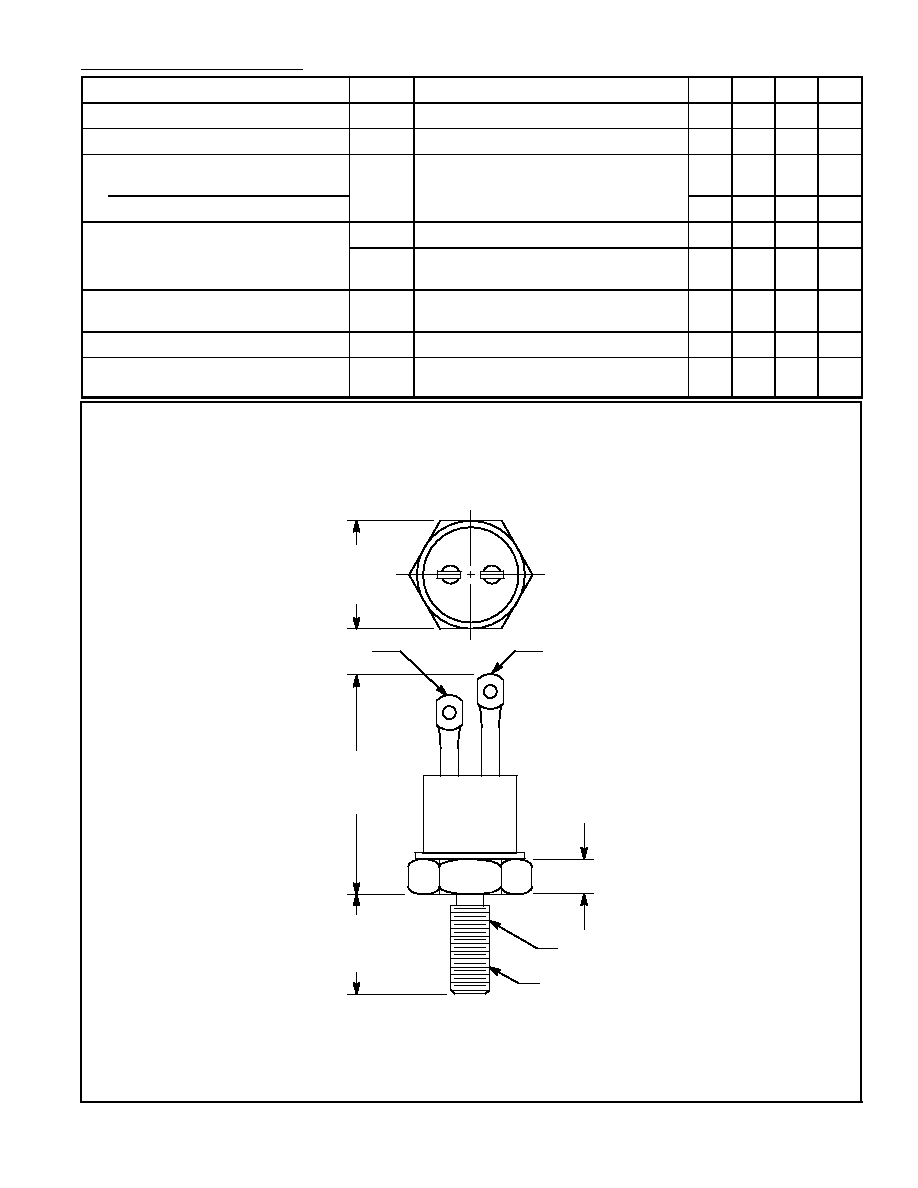
.125 (3.17) Max
.431
(10.98
Max
.855
(21.7)
Max
.453
(111.5)
Max
10≠32 UNF≠2A
MT
2
MT
1
Gate