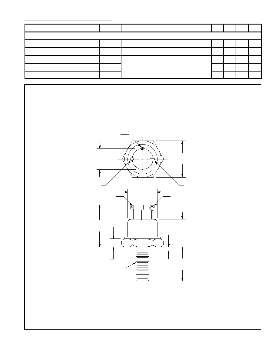
NTE70
Silicon NPN Transistor
High Voltage Power Amp, Switch
Description:
The NTE70 is a silicon NPN transistor in a TO63 type case utilizing C2R processing which describes
a manufacturing technology that provides surface stabilization for high voltage operation and en-
hances long term reliability.
Absolute Maximum Ratings:
Collector≠Base Voltage, V
CBO
180V
. . . . . . . . . . . . . . . . . . . . . . . . . . . . . . . . . . . . . . . . . . . . . . . . . . . . . .
Collector≠Emitter Voltage, V
CEO
150V
. . . . . . . . . . . . . . . . . . . . . . . . . . . . . . . . . . . . . . . . . . . . . . . . . . . . .
Emitter≠Base Voltage, V
EBO
6V
. . . . . . . . . . . . . . . . . . . . . . . . . . . . . . . . . . . . . . . . . . . . . . . . . . . . . . . . . .
Continuous Collector Current, I
C
20A
. . . . . . . . . . . . . . . . . . . . . . . . . . . . . . . . . . . . . . . . . . . . . . . . . . . . .
Continuous Base Current, I
B
20A
. . . . . . . . . . . . . . . . . . . . . . . . . . . . . . . . . . . . . . . . . . . . . . . . . . . . . . . . .
Total Power Dissipation (T
C
= +25
∞
C), P
D
250W
. . . . . . . . . . . . . . . . . . . . . . . . . . . . . . . . . . . . . . . . . . .
Operating Junction Temperature Range, T
J
≠65
∞
to +200
∞
C
. . . . . . . . . . . . . . . . . . . . . . . . . . . . . . . . . .
Storage Temperature Range, T
stg
≠65
∞
to +200
∞
C
. . . . . . . . . . . . . . . . . . . . . . . . . . . . . . . . . . . . . . . . . .
Thermal Resistance, Junction≠to≠Case, R
thJC
0.7
∞
C/W
. . . . . . . . . . . . . . . . . . . . . . . . . . . . . . . . . . . . .
Electrical Characteristics: (T
C
= +25
∞
C unless otherwise specified)
Parameter
Symbol
Test Conditions
Min
Typ Max Unit
OFF Characteristics
Collector≠Emitter Breakdown Voltage
V
(BR)CEO
I
C
= 50mA
150
≠
≠
V
Emitter Cutoff Current
I
EBO
V
EB
= 6V
≠
≠
100
µ
A
Collector Cutoff Current
I
CEX
V
CE
= Rated V
CB
, V
EB
= 1.5V
≠
≠
10
µ
A
V
CE
= Rated V
CB
, V
EB
= 1.5V, T
C
= +150
∞
C
≠
≠
1.0
mA
ON Characteristics (Note 1)
DC Current Gain
h
FE
V
CE
= 4V, I
C
= 20A
50
≠
≠
Collector≠Emitter Saturation Voltage
V
CE(sat)
I
C
= 50A, I
B
= 10A
≠
≠
3.0
V
Base≠Emitter Saturation Voltage
V
BE(sat)
I
C
= 20A, I
B
= 2A
≠
≠
1.8
V
I
C
= 50A, I
B
= 10A
≠
≠
3.5
V
Note 1. Pulse Test: Pulse Width = 300
µ
s, Duty Cycle
2%.