
NTE7049
Integrated Circuit
CMOS≠Sync Generator for TV & Video
Processing Systems
Description:
The NTE7049 is a CMOS LSI sync generator in a 24≠Lead DIP type package that produces all the timing sig-
nals required to drive a fully 2≠to≠1 interlaced 525≠line 30≠frame/second, or 625≠line 25≠frame/second TV
camera or video processing system. A complete sync waveform is produced which begins each field with six
serrated vertical sync pulses, preceded and followed by six half≠width double frequency equalizing pulses.
The sync output is gated by the master clock to preserve horizontal phase continuity during the vertical interval.
The NTE7049 can be operated either in "genlock" mode, in which it is synchronized with a reference sync pulse
train from another TV camera, or in "stand≠alone" mode, in which it is synchronized with a local on≠chip crystal
oscillator (the crystal and two passive components are off chip). Also, the circuit can sense the presence or
absence of a reference sync pulse train and automatically select the "genlock" or "stand≠alone" mode.
A frame sync pulse is produced at the beginning of every odd field. The vertical counter can be reset to either
the first equalizing pulse or the first vertical sync pulse of the vertical interval.
Features:
D
Interlaced Composite Sync Output
D
Automatic Genlock Capability
D
Crystal Oscillator Operation
D
525 or 625 Line Operation
D
Vertical Reset Option
D
Wide Power Supply Operating Voltage: 4V to 15V
Applications:
D
Cameras
D
Monitors and Displays
D
CATV
D
Teletext
D
Video Games
D
Sync Restorer
D
Video Service Instruments
Absolute Maximum Ratings:
DC Supply Voltage (Voltage referenced to V
SS
terminal), V
DD
15V
. . . . . . . . . . . . . . . . . . . . . . . . . . . . . . . . . . . .
Input Voltage Range (All Inputs), V
I
V
SS
V
I
V
DD
. . . . . . . . . . . . . . . . . . . . . . . . . . . . . . . . . . . . . . . . . . . . . . . . .
DC Input Current (Any One Input), I
I
±
10mA
. . . . . . . . . . . . . . . . . . . . . . . . . . . . . . . . . . . . . . . . . . . . . . . . . . . . . . .
Power Dissipation (T
A
= ≠40
∞
to +60
∞
C), P
D
500mW
. . . . . . . . . . . . . . . . . . . . . . . . . . . . . . . . . . . . . . . . . . . . . . . .
Derate Linearly Above +60
∞
C to 200mW
12mW/
∞
C
. . . . . . . . . . . . . . . . . . . . . . . . . . . . . . . . . . . . . . . . . . .
Device Dissipation Per Output Transistor (T
A
= ≠40
∞
to +85
∞
C)
100mW
. . . . . . . . . . . . . . . . . . . . . . . . . . . . . . . .
Operating Temperature Range, T
A
≠40
∞
to +85
∞
C
. . . . . . . . . . . . . . . . . . . . . . . . . . . . . . . . . . . . . . . . . . . . . . . . . . .
Storage Temperature Range, T
stg
≠65
∞
to +150
∞
C
. . . . . . . . . . . . . . . . . . . . . . . . . . . . . . . . . . . . . . . . . . . . . . . . . .
Lead Temperature (During Soldering, 1/16
±
1/32 from case for 10sec), T
L
+265
∞
C
. . . . . . . . . . . . . . . . . . . . . .
Static Electrical Characteristics: (T
A
= +25
∞
C unless otherwise specified)
Parameter
Symbol
Test Conditions
Min
Typ
Max
Unit
Quiescent Device Current
I
DD
V
DD
= 5V
0.5
0.75
1.0
mA
V
DD
= 10V
1.5
2.0
2.5
mA
V
DD
= 15V
3.0
4.0
5.0
mA
Output Voltage, Low Level
V
OL
V
DD
= 5V
≠
≠
0.01
V
V
DD
= 10V
≠
≠
0.01
V
Output Voltage, High Level
V
OH
V
DD
= 5V
4.99
≠
≠
V
V
DD
= 10V
9.99
≠
≠
V
Threshold Voltage, N≠Channel
V
TH
N
I
D
= 10
µ
A
1.0
1.5
2.6
V
Threshold Voltage, P≠Channel
V
TH
P
I
D
= 10
µ
A
≠1.0
≠1.5
≠2.6
V
Noise Immunity (Any Input)
Low Level
V
NL
V
DD
= 5V
1.5
2.25
≠
V
V
DD
= 10V
3.0
4.5
≠
V
High Level
V
NH
V
DD
= 5V
1.5
2.25
≠
V
V
DD
= 10V
3.0
4.5
≠
V
Output SINK Current, N≠Channel
I
D
N
V
DD
= 5V
V
O
= 0.5V
80
160
≠
µ
A
V
O
= 5V
960
1920
≠
µ
A
V
DD
= 10V
V
O
= 0.5V
200
400
≠
µ
A
V
O
= 10V
2400
4800
≠
µ
A
Output SOURCE Current, P≠Channel
I
D
P
V
DD
= 5V
V
O
= 4.5V
80
160
≠
µ
A
V
O
= 0V
960
1920
≠
µ
A
V
DD
= 10V
V
O
= 9.5V
200
400
≠
µ
A
V
O
= 0V
2400
4800
≠
µ
A
Input Current (Each Input)
I
I
≠
10
≠
pA
Dynamic Electrical Characteristics: (T
A
= +25
∞
C, C
L
= 15pF, Note 1 unless otherwise specified)
Parameter
Symbol
Test Conditions
Min
Typ
Max
Unit
Output State
Propagation Delay Time
(50% to 50%)
Low≠to≠High Level
t
PLH
V
DD
= 5V
≠
40
80
ns
High≠to≠Low Level
t
PHL
V
DD
= 10V
≠
20
40
ns
Transition Time
(10% to 90%)
Low≠to≠High
t
TLH
V
DD
= 5V
≠
45
90
ns
High≠to≠Low
t
THL
V
DD
= 10V
≠
30
60
ns
Input Capacity (Per Input)
C
I
≠
5
≠
pF
Note 1. Typical temperature coefficient for all values of V
DD
= 0.3%/
∞
C.
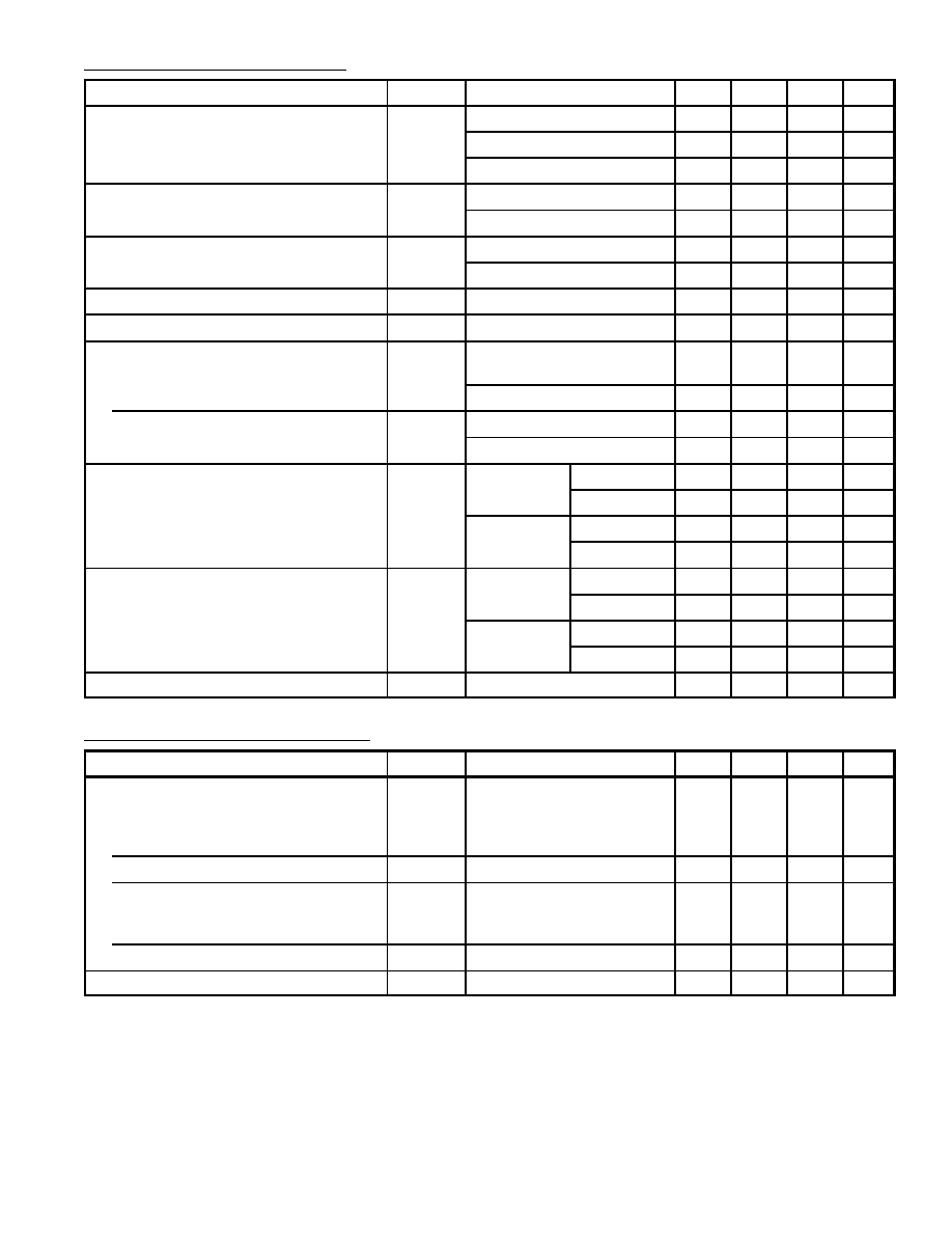
Pin Connection Diagram
V
DD
V
SS
V
SS
Mixed Beam Blanking Output
Horizontal Drive Output
Mixed Processing Blanking Output
Delay, Genlock to Crystal OSC
R/C Connection for Genlock OSC
Master Frequency Input
Crystal OSC Feedback Tap
Delay, Genlock to Crystal OSC
Short Vertical Drive Output
Mixed Sync Output
Vertical Drive Output
Horizontal Clamp Output
Resistor Connection for Genlock OSC
Horizontal Processing Blanking Output
Genlock Input (Composite Sync)
Genlock OSC Capacitor Connection
Vertical Reset to
Vertical Counter Reset
525 Line to 625 Line Operation Switch
1
2
3
4
5
6
7
24
23
22
21
20
19
18
8
9
17
Vertical Processing Blanking Output
16
Frame Sync Output (Odd Field)
10
11
12
15
14
13
to First Equalizing Pulse
First Vertical Sync Pulse
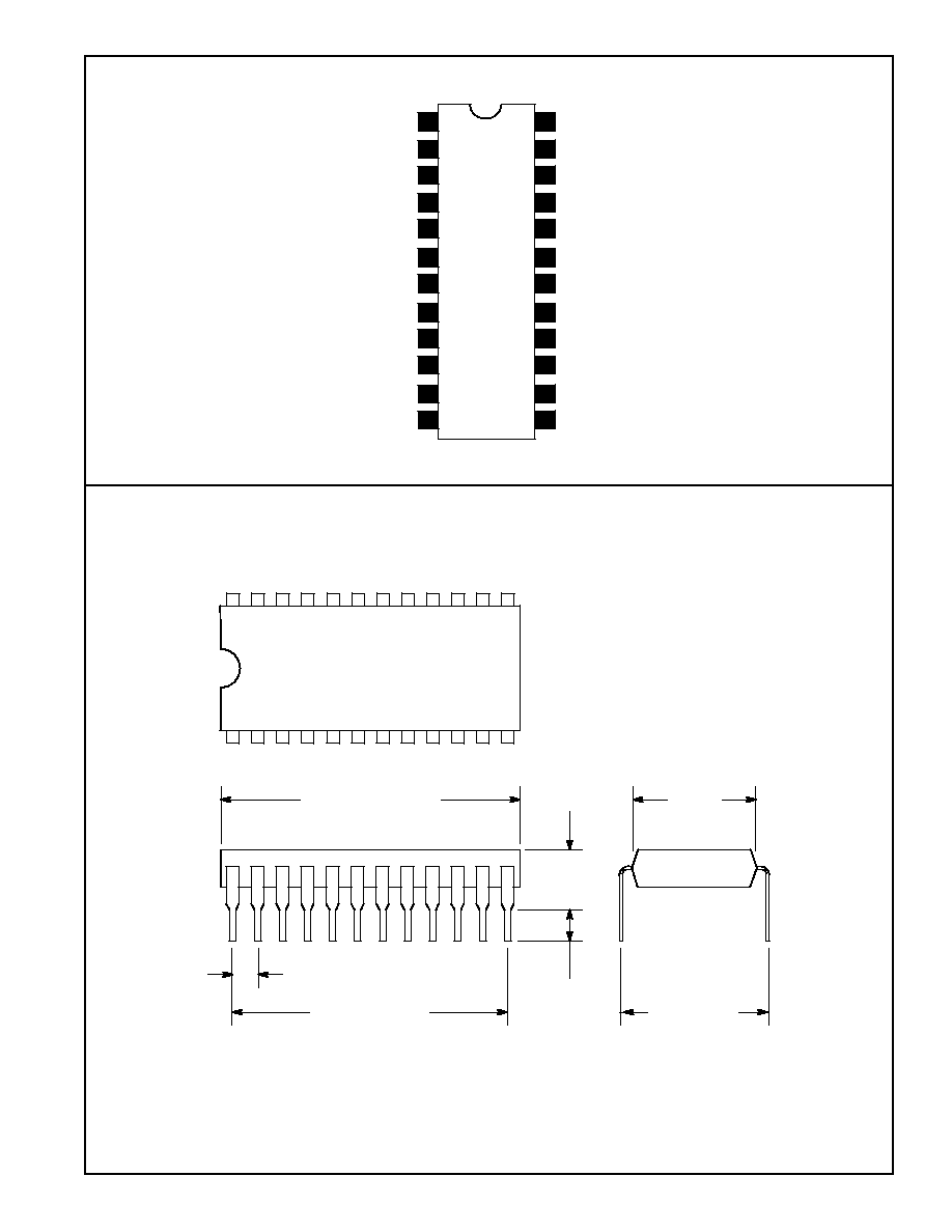
1
12
24
13
1.300 (33.02) Max
.520
(13.2)
.600 (15.24)
1.100 (27.94)
.100 (2.54)
.225
(5.73)
Max
.126
(3.22)
Min