 | –≠–ª–µ–∫—Ç—Ä–æ–Ω–Ω—ã–π –∫–æ–º–ø–æ–Ω–µ–Ω—Ç: NTE7116 | –°–∫–∞—á–∞—Ç—å:  PDF PDF  ZIP ZIP |

NTE7116
Integrated Circuit
Phase Lock Loop (PLL) Stereo Decoder
(BTSC System)
Description:
The NTE7116 is a phase lock loop (PLL) stereo decoder in a 20≠Lead DIP type package designed
primarily for low cost stereo decoding in a low≠to≠medium≠line TV. The MUX input (Pin1) is a low
impedance current input, the gain of the input amplifier is therefore determined by the external resistor
R1. All characteristics are measured with R1 = 47k
. The de≠emphasis of (L, R) and (L ≠ R) can
be chosen by means of external capacitors and resistors. The supply voltage range of the device is
from 7V to 16V.
Features:
D
Wide Supply Voltage Range
D
Automatic Mono/Stereo Switching (Pilot Presence Detector)
D
LED Driver for Stereo Indicator
D
Smooth Mono/Stereo Control
D
Matrix and Two Amplifiers for Left and Right Output Signals
D
A Source Selector to Switch between the MUX Signal and an External Signal
D
Mute Circuit for 60dB Muting of the Output Level
D
External De≠Emphasis Control of (L, R) and (L ≠ R)
D
6dB Fixed Attenuation of (L ≠ R) with respect to (L + R) Prior to Matrix
D
All Pins are Protected Against Electrostatic Discharge (ESD)
Absolute Maximum Ratings:
Supply Voltage Range (Pin5), V
P
18V
. . . . . . . . . . . . . . . . . . . . . . . . . . . . . . . . . . . . . . . . . . . . . . . . . . . . .
LED Driver Current (Peak Value), I
3
75mA
. . . . . . . . . . . . . . . . . . . . . . . . . . . . . . . . . . . . . . . . . . . . . . . .
Total Power Dissipation (T
A
= +25
∞
C), P
tot
1.9W
. . . . . . . . . . . . . . . . . . . . . . . . . . . . . . . . . . . . . . . . . . . .
Electrostatic Handling, V
es
≠2 to +2kV
. . . . . . . . . . . . . . . . . . . . . . . . . . . . . . . . . . . . . . . . . . . . . . . . . . . . .
Operating Ambient Temperature Range, T
A
0
∞
to +70
∞
C
. . . . . . . . . . . . . . . . . . . . . . . . . . . . . . . . . . . . .
Storage Temperature Range, T
stg
≠65
∞
to +150
∞
C
. . . . . . . . . . . . . . . . . . . . . . . . . . . . . . . . . . . . . . . . . .
DC Characteristics:
(V
S
= 8.5V, T
A
= +25
∞
C, all voltages are with respect to GND (Pin20), all
currents are positive into the device unless otherwise specified)
Parameter
Symbol
Test Conditions
Min
Typ
Max
Unit
Supply Voltage
V
S
7.0
8.5
16.0
V
Total Current Consumption
I
tot
Without LED Driver
≠
19
25
mA
Power Dissipation
P
tot
≠
160
≠
mW
Voltage
Pin1
V
1
≠
2.1
≠
V
Pins 8, 9, 10, 11, 12, & 13
V
8≠13
≠
4.2
≠
V
DC Output Current (Pin14 & Pin15)
≠I
14
, I
15
1.1
1.4
1.8
mA
LED Driver Current (Pin3)
I
3
≠
≠
20
mA
Switch "VCO≠OFF" Voltage
V
19
I
19
= 50
µ
A
≠
2
≠
V
Switch "VCO≠OFF" Current
I
19
50
≠
≠
µ
A
AC Characteristics:
(V
S
= 8.5V, T
A
= +25
∞
C, AC Conditions: (1) Input signal (V
i
) of 815mV
P≠P
for
L = 1, R = 1 (mono), f
m
= 1kHz (80% modulation); (2) MUX input signal (V
i
)
of 1.2V
P≠P
for L = 1, R = 0 and no dbx, f
m
= 1kHz (stereo) and V
pilot
= 200V
P≠P
;
(3) S1 open, unless specified (without L ≠ R filter), VCO measured with an
external IF roll≠off network (≠2dB at 31.5kHz = 2f
H
) at the input. All the above
conditions apply unless otherwise specified)
Parameter
Symbol
Test Conditions
Min
Typ
Max
Unit
Overall Performance V
i
to V
o
Input Current (rms)
I
(rms)
≠
≠
12
µ
A
Overall gain
G
O
Mono; R1 = 47k
4.0
5.8
7.0
dB
AF Output Voltage (rms)
V
11
= V
10
460
560
640
mV
V
15
= V
14
≠
245
≠
mV
Total Harmonic Distortion
THD
Note 1
≠
0.3
0.5
%
Output Voltage
V
11
= V
10
THD = 1%
≠
800
≠
mV
Output Channel Unbalance
V
11
/V
10
≠
0.1
1.0
dB
Channel Separation
L = 1, R = 0
24
28
≠
dB
Signal to Noise Ratio
S/N
Bandwidth 20Hz to 16kHz
≠
76
≠
dB
Pilot Presence Detector (Note 2)
Switching to
Stereo
V
pilot
≠
40
60
mV
Mono
15
30
≠
mV
Hysteresis
V
pilot
≠
2.5
≠
dB
Channel Separation
Full Stereo
V
16
1.25V
24
28
≠
dB
Smooth Operation
V
16
= 1V Typ
≠
10
≠
dB
Attenuation (L ≠ R)
≠
6
≠
dB
Note 1. Guaranteed for mono, mono + pilot and stereo.
Note 2. Adjustable.

AC Characteristics (Cont'd): (V
S
= 8.5V, T
A
= +25
∞
C, AC Conditions: (1) Input signal (V
i
) of
815mV
P≠P
for L = 1, R = 1 (mono), f
m
= 1kHz (80% modulation); (2)
MUX input signal (V
i
) of 1.2V
P≠P
for L = 1, R = 0 and no dbx, f
m
= 1kHz
(stereo) and V
pilot
= 200V
P≠P
; (3) S1 open, unless specified (without
L ≠ R filter), VCO measured with an external IF roll≠off network (≠2dB
at 31.5kHz = 2f
H
) at the input. All the above conditions apply unless
otherwise specified)
Parameter
Symbol
Test Conditions
Min
Typ
Max Unit
Carrier & Harmonic Suppression at the Output (Note 3)
Pilot Signal Suppression
f
H
f
pilot
= 15.734kHz (1f
H
)
32
36
≠
dB
Subcarrier Suppression
2f
H
f = 2f
H
≠
60
≠
dB
VCO Suppression
12f
H
f = 12f
H
≠
75
≠
dB
SAP Signal Suppression
(Second Audio Program)
5f
H
f = 5f
H
≠
60
≠
dB
Intermodulation Suppression
f
m
= 8.367kHz
2
Spurious Signal, f
s
= 1kHz
≠
80
≠
dB
f
m
= 10.832kHz
3
Spurious Signal, f
s
= 1kHz
≠
70
≠
dB
Ripple Rejection
RR
120
f = 120Hz, V
ripple
= 100mV, mono
≠
50
≠
dB
Voltage Controlled Oscillator (VCO)
R Adjust (R5)
R
adj
f
OSC
= 188.808kHz,
R7 = 10k
5%, C6 = 820pF 1%
0
≠
8
k
Capture Range
f/f
Deviation from f
OSC
center
frequency: V
pilot
= 200mV
P≠P
≠
45
≠
%
Temperature Coefficient
TC
Uncompensated
≠
250 x 10
≠6
≠
K
≠1
Output Amplifiers
Gain
MUX
G
V
6.7
7.2
7.7
dB
External Signal
≠0.5
0
+0.5
dB
Input Impedance
Z
i
≠
50
≠
k
Output Impedance
Z
o
≠
10
≠
External Load Impedance
Z
1
10
≠
≠
k
External Load Capacitance
Z
1
≠
≠
1.5
nF
Mute Suppression
MUX Signal
56
60
≠
dB
External Signal
56
60
≠
dB
DC Offset Voltage at Outputs
V
Mute OFF≠to≠ON
≠
10
50
mV
Mute ON≠to≠OFF
≠
10
50
mV
Source Selector (Pin6)
Suppression of MUX Signal
V
6
2V
80
90
≠
dB
Suppression of External Signal
V
6
0.8V
56
60
≠
dB
Switching Level (MUX Selected)
Voltage
V
IL
≠
≠
0.8
V
Current
I
IL
V
i
= 0.8V
≠
10
25
µ
A
Note 3. S1 closed; reference: AF output voltage f = 1kHz mono.
AC Characteristics (Cont'd): (V
S
= 8.5V, T
A
= +25
∞
C, AC Conditions: (1) Input signal (V
i
) of
815mV
P≠P
for L = 1, R = 1 (mono), f
m
= 1kHz (80% modulation); (2)
MUX input signal (V
i
) of 1.2V
P≠P
for L = 1, R = 0 and no dbx, f
m
= 1kHz
(stereo) and V
pilot
= 200V
P≠P
; (3) S1 open, unless specified (without
L ≠ R filter), VCO measured with an external IF roll≠off network (≠2dB
at 31.5kHz = 2f
H
) at the input. All the above conditions apply unless
otherwise specified)
Parameter
Symbol
Test Conditions
Min
Typ
Max Unit
Source Selector (Cont'd) (Pin6)
Switching Level (External Selected)
Voltage
V
IH
2
≠
V
P
V
Current
I
IH
V
i
= V
P
≠
0.1
1.0
µ
A
Muting Circuit (Pin7)
Input Voltage
V
IL
Mute ON
≠
≠
0.8
V
V
IH
Mute OFF
2
≠
V
P
V
Input Current
≠I
IL
Mute ON, V
IL
= 0.8V
≠
10
25
µ
A
I
IL
Mute OFF, V
IH
= V
P
≠
0.1
1.0
µ
A
Note 4. Intermodulation suppression (Beat Frequency Components (BFC)):
2
=
V
O
(signal) (at 1kHz)
V
O
(spurious) (at 1kHz)
; f
s
= (2 x 8.367kHz) ≠f
H
3
=
V
O
(signal) (at 1kHz)
V
O
(spurious) (at 1kHz)
; f
s
= (3 x 10.823kHz) ≠2f
H
measured with 100% modulated input signal: L = R; pilot signal = 200mV
P≠P
; f
m
= 8.367 or
10.823kHz.
V
O
Left
V
O
Decoder Right De≠Emphasis
V
O
Decoder Left De≠Emphasis
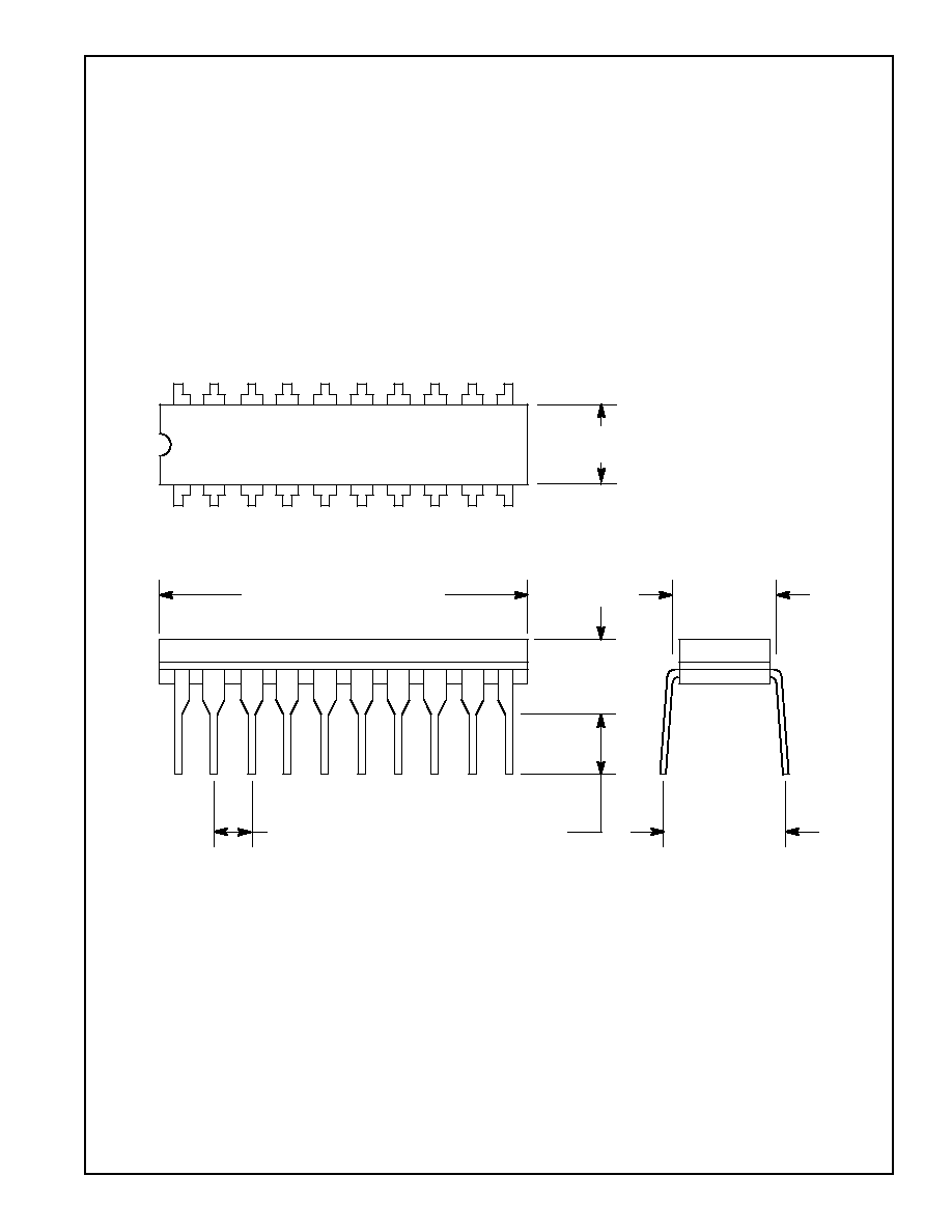
Pin Connection Diagram
V
O
Right
V
P
Input 1, Left
Input 2, Right
1
2
3
4
Multiplexer Input
Pilot Presence Det
LED Driver Output
VCO
5
6
Source Selector Input
7
Mute Input
8
Input 2, Left
20
19
18
17
GND
Phase Det
L≠R De≠Emphasis
L≠R De≠Emphasis
16
Smooth Mono/Stereo Control
15
14
13
Input 1, Right
9
12
10
11
.995 (25.3) Max
.280 (7.12) Max
.100 (2.54)
.125 (3.17) Min
.385 (9.8)
.300
(7.62)
.280
(7.12)
1
10
20
11