 | ÐлекÑÑоннÑй компоненÑ: NTE7134 | СкаÑаÑÑ:  PDF PDF  ZIP ZIP |
Äîêóìåíòàöèÿ è îïèñàíèÿ www.docs.chipfind.ru

NTE7134
Integrated Circuit
Horizontal and Vertical Deflection Controller
for Monitors
Description:
The NTE7134 is a high performance and efficient solution for autosync monitors in a 32Lead DIP
type package. The concept is fully DC controllable and can be used in applications with a microcon-
troller and standalone in rock bottom solutions.
This device provides synchronization processing, H + V synchronization with full autosync capability,
and very short setting times after mode changes. External power components are givena great deal
of protection. The IC generates the drive waveforms for DCcoupled vertical boosters.
The NTE7134 provides ectended functions e.g. as a flexible SMPS block and an extensive set of ge-
ometry control facilities, providing excellent picture quality.
Features:
Concept Features
D
Full Horizontal (H) Plus Vertical (V) Autosync Capability
D
Completely DC Controllable for Analog and Digital Concepts
D
Excellent Geometry Control Functions (e.g. Automatic Correction of EastWest (EW) Parabola
During Adjustment of Vertical Size and Vertical Shift)
D
Felxible Switched Mode Power Supply (SMPS) Function Block for Feedback and Feed Forward
Converters.
D
XRay Protection
D
StartUp and SwitchOff Sequences for safe Operation of All Power Components
D
Very Good Vertical Linearity
D
Internal Supply Voltage Stabilization
Synchronization Inputs
D
Can Handle All Sync Signals (Horizontal, Vertical, Composite and SyncOnVideo)
D
Combined Output for Video Clamping, Vertical Blanking and Protection Blanking
D
Start of Video Clamping Pulses Externally Selectable
Horizontal Section
D
Extremely Low Jitter
D
Frequency Locked Loop for Smooth Catching of Line Frequrncy
D
Simple Frequency Preset of f
min
and f
max
by External Resistors
D
DC Controllable Wdie Range Linear Picture Position
D
Soft Start for Horizontal Driver
Vertical Section
D
Vertical Amplitude Independent of Frequency
D
DC Controllable Picture Height, Picture Position and SCorrection
D
Differential Current Outputs for DC Coupling to Vertical Booster
Features (Cont'd):
EW Section
D
Output for DC Adjustable EW Parabola
D
DC Controllable Picture Width and Trapezium Correction
D
Optional Tracking of EW Parabola with Line Frequency
D
Prepared for Additional DC Controls of Vertical Linearity, EWCorner, EW Pin Balance, EW
Parallelogram, Vertical Focus by Extended Application
Absolute Maximum Ratings: (All voltages measured with respect to GND)
Supply Voltage (Pin9), V
CC
0.5 to +16V
. . . . . . . . . . . . . . . . . . . . . . . . . . . . . . . . . . . . . . . . . . . . . . . . . .
Input Voltages, V
I(n)
Pin5
0.5 to +6.0V
. . . . . . . . . . . . . . . . . . . . . . . . . . . . . . . . . . . . . . . . . . . . . . . . . . . . . . . . . . . . . . .
Pin15, Pin17, Pin18, Pin19, Pin23, Pin28, Pin30
0.5 to +6.5V
. . . . . . . . . . . . . . . . . . . . . . . .
Pin2
0.5 to +8.0V
. . . . . . . . . . . . . . . . . . . . . . . . . . . . . . . . . . . . . . . . . . . . . . . . . . . . . . . . . . . . . . .
Pin10
0.5 to +16V
. . . . . . . . . . . . . . . . . . . . . . . . . . . . . . . . . . . . . . . . . . . . . . . . . . . . . . . . . . . . . . .
Output Voltages, V
O(n)
Pin12, Pin13
0.5 to +6.5V
. . . . . . . . . . . . . . . . . . . . . . . . . . . . . . . . . . . . . . . . . . . . . . . . . . . . . . . .
Pin6, Pin7
0.5 to +16V
. . . . . . . . . . . . . . . . . . . . . . . . . . . . . . . . . . . . . . . . . . . . . . . . . . . . . . . . . . .
Input/Output Voltages, V
IO(n)
Pin3, Pin4
0.5 to +6.0V
. . . . . . . . . . . . . . . . . . . . . . . . . . . . . . . . . . . . . . . . . . . . . . . . . . . . . . . . . .
Pin14
0.5 to +6.5V
. . . . . . . . . . . . . . . . . . . . . . . . . . . . . . . . . . . . . . . . . . . . . . . . . . . . . . . . . . . . . .
Horizontal Driver Output Current, I
HDRV
10 to +10mA
. . . . . . . . . . . . . . . . . . . . . . . . . . . . . . . . . . . . . .
Horizontal Flyback Input Current, I
HFLB
100mA
. . . . . . . . . . . . . . . . . . . . . . . . . . . . . . . . . . . . . . . . . . . . .
Video Clamping Pulse/Vertical Blanking Output Current, I
CLBL
10mA
. . . . . . . . . . . . . . . . . . . . . . . .
B+ Control OTA Output Current, I
BOP
1mA
. . . . . . . . . . . . . . . . . . . . . . . . . . . . . . . . . . . . . . . . . . . . . . . .
B+ Control Driver Output Current, I
BDRV
50mA
. . . . . . . . . . . . . . . . . . . . . . . . . . . . . . . . . . . . . . . . . . . . .
EW Driver Output Current, I
EWDRV
5mA
. . . . . . . . . . . . . . . . . . . . . . . . . . . . . . . . . . . . . . . . . . . . . . . . . .
Electrostatic Discharge for All Pins (Note 1), V
esd
Machine Model
±
400V
. . . . . . . . . . . . . . . . . . . . . . . . . . . . . . . . . . . . . . . . . . . . . . . . . . . . . . . . . . . .
Human Body Model
±
3000V
. . . . . . . . . . . . . . . . . . . . . . . . . . . . . . . . . . . . . . . . . . . . . . . . . . . . . . .
Operating Junction Temperature, T
J
+150
°
C
. . . . . . . . . . . . . . . . . . . . . . . . . . . . . . . . . . . . . . . . . . . . . . .
Operating Ambient Temperatrure Range, T
A
0
°
to +70
°
C
. . . . . . . . . . . . . . . . . . . . . . . . . . . . . . . . . . . .
Storage Temperature Range, T
stg
55
°
to +150
°
C
. . . . . . . . . . . . . . . . . . . . . . . . . . . . . . . . . . . . . . . . . .
Thermal Resistance, JunctiontoAmbient (In Free Air), R
thJA
55K/W
. . . . . . . . . . . . . . . . . . . . . . . .
Note 1. Machine model: 200pF, 25
, 2.5
µ
H; Human body model: 100pF, 1500
, 7.5
µ
H.
Electrical Characteristics: (V
P
= 12V, T
A
= +25
°
C unless otherwise specified)
Parameter
Symbol
Test Conditions
Min
Typ
Max
Unit
Horizontal Sync Separator
Input Characteristics for DCCoupled TTL Signals [HSYNC (Pin15)]
Sync Input Signal Voltage
V
DC(HSYNC)
1.7
V
Slicing Voltage Level
1.2
1.4
1.6
V
Rise Time of Sync Pulse
t
r(HSYNC)
10
500
ns
Fall Time of Sync Pulse
t
f(HSYNC)
10
500
ns
Minimum Width of Sync Pulse
t
W(HSYNC)
0.7
µ
s
Input Current
I
DC(HSYNC)
V
HSYNC
= 0.8V
200
µ
A
V
HSYNC
= 5.5V
µ
A
Electrical Characteristics (Cont'd): (V
P
= 12V, T
A
= +25
°
C unless otherwise specified)
Parameter
Symbol
Test Conditions
Min
Typ
Max
Unit
Horizontal Sync Separator (Cont'd)
Input Characteristics for ACCoupled Video Signals (SynconVideo, Negative Sync Polarity)
Sync Amplitude of Video Input Signal
Voltage
V
AC(HSYNC)
300
mV
Slicing Voltage Level
(Measured from Top Sync)
R
S
= 50
90
120
150
mV
Top Sync Clamping Level
V
clamp(HSYNC)
1.1
1.28
1.5
V
Charge Current for Coupling Capacitor
I
C(HSYNC)
V
HSYNC
> V
clamp(HSYNC)
1.7
2.4
3.4
µ
A
Minimum Width of Sync Pulse
t
HSYNC(min)
0.7
µ
s
Maximum Source Resistance
R
S(max)
Duty factor = 7%
1500
Differential Input Resistance
r
diff(HSYNC)
During Sync
80
Automatic Polarity Correction for Horizontal Sync
Horizontal Sync Pulse Width Related to t
H
t
p(H)
f
H
< 45kHz
20
%
t
H
f
H
> 45kHz
25
&
Delay Time for Changing Polarity
t
p(H)
0.3
1.8
ms
Vertical Sync Integrator
Integration Time for Generation of a
Vertical Trigger Pulse
t
int(V)
f
H
= 31.45kHz,
I
HREF
= 1.052mA
7.0
10.0
13.0
µ
s
f
H
= 64kHz,
I
HREF
= 2.141mA
3.9
5.7
6.5
µ
s
f
H
= 100kHz,
I
HREF
= 3.345mA
2.5
3.8
4.5
µ
s
Vertical Sync Slicer (DCCoupled, TTL Compatible) [VSYNC (Pin14)]
Sync Input Signal Voltage
V
VSYNC
1.7
V
Slicing Voltage Level
1.2
1.4
1.6
V
Input Current
I
VSYNC
0V < V
SYNC
< 5.5V
±
10
µ
A
Vertical Sync Output at VSYNC (Pin14) During Composite Sync at HSYNC (Pin15)
Output Current
I
VSYNC
During Internal Vertical Sync
0.7
1.0
1.35
mA
Internal Clamping Voltage Level
V
VSYNC
During Internal Vertical Sync
4.4
4.8
5.2
V
Steepness of Slopes
300
ns/mA
Automatic Polarity Correction for Vertical Sync
Maximum Width of Vertical Sync Pulse
t
VSYNC(max)
300
µ
s
Delay for Change Polarity
t
d(VPOL)
0.3
1.8
ms
Video Clamping/Vertical Blanking Output [CLCB (Pin16)]
Width of Video Clamping Pulse
t
clamp(CLBL)
Measured at V
CLBL
= 3V
0.6
0.7
0.8
µ
s
Temperature Coefficient of V
clamp(CLCB)
TC
clamp
+4
mV/K
Steepness of Slopes for Clamping Pulse
R
L
= 1M
, C
L
= 20pF
50
ns/V
Top Voltage Level of Vertical
Blanking Pulse
V
blank(CLBL)
Note 2
1.7
1.9
2.1
V
Width of Vertical Blanking Pulse
t
blank(CLBL)
240
300
360
µ
s
Note 2. Continuous blanking at CLCB (Pin16) will be activated, if one of the following conditions is true:
a) No horizontal flyback pulse at HFLB (Pin1) within a line
b) Xray protection is triggered
c) Voltage at HPLL2 (Pin31) is low (for soft start of horizontal drive)
d) Supply voltage at V
VV
(Pin9) is low
e) PLL1 unlocked while frequencylocked loop is in search mode
Electrical Characteristics (Cont'd): (V
P
= 12V, T
A
= +25
°
C unless otherwise specified)
Parameter
Symbol
Test Conditions
Min
Typ
Max
Unit
Video Clamping/Vertical Blanking Output (Cont'd) [CLCB (Pin16)]
Temperature Coefficient of V
blank(CLBL)
TC
blank
+2
mV/K
Output Voltage During Vertical Scan
V
scan(CLBL)
I
CLBL
= 0
0.59
0.63
0.67
V
Temperature Coefficient of V
scan(CLBL)
TC
scan
2
mV/K
Internal Sink Current
I
sink(CLBL)
2.4
mA
External Load Current
I
load(CLBL)
3.0
mA
Selection of Leading/Trailing Edge for Video Clamping Pulse
Voltage at CLSEL (Pin10) for Trigger with
Leading Edge of Horizontal Sync
V
CLSEL
7
V
CC
V
Voltage at CLSEL (Pin10) for Trigger with
Trailing Edge of Horizontal Sync
0
5
V
Delay Between Leading Edge of
Horizontal Sync and Start of
Horizontal Clamping Pulse
t
d(clamp)
V
CLSEL
> 7V
300
ns
Delay Between Leading Trailing of
Horizontal Sync and Start of
Horizontal Clamping Pulse
V
CLSEL
< 5V
130
ns
Maximum Duration of Video Clamping
t
clamp(max)
V
CLBL
= 3V, V
CLSEL
> 7V
0.15
µ
s
Pulse After End of Horizontal Sync
V
CLBL
= 3V, V
CLSEL
> 5V
1.0
µ
s
Input Resistance at CLSEL (Pin10)
R
CLSEL
V
CLSEL
V
CC
80
k
PLL1 Phase Comparator and FrequencyLocked Loop [HPLL1 (Pin26) and HBUF (Pin27)]
Maximum Width of Horizontal Sync Pulse
t
HSYNC(max)
f
H
< 45kHz, Note 2
20
&
(Referenced to Line Period)
f
H
> 45kHz, Note 3
25
%
Total LockIn Time of PLL1
t
lock(HPLL1)
40
80
ms
Control Voltage
V
HPLL1
Note 4, Note 5
Buffered f/v Voltage at HBUF (Pin27)
V
HBUF
f
H(min)
, Note 6
5.6
V
f
H(max)
, Note 6
2.5
V
Maximum Load Current
I
load(HBUF)
4.0
mA
Adjustment of Horizontal Picture Position
Horizontal Shift Adjustment Range
HPOS
I
HSHIFT
= 0
10.5
%
(Referenced to Horizontal Period)
I
HSHIFT
= 135
µ
A
+10.5
%
Input Current
I
HPOS
HPOS = +10.5%
110
120
135
µ
A
HPOS = 10.5%
0
µ
A
Note 3. To ensure safe locking of the horizontal oscillator, one of the following procedures is required:
a) Search mode starts always from f
min
. Then the PLL1 filter components are a 3.3nF
capacitor from Pin26 to GND in parallel with an 8.2k
resistor in series with a 47nF
capacitor.
b) Search mode starts either from f
min
or f
max
with HPOS in middle position (I
HPOS
= 60
µ
A).
Then the PLL1 filter components are a 1.5nF capacitor from Pin26 to GND in parallel
with a 27k
resistor in series with a 47nF capacitor.
c) After locking is achieved, HPOS can be operated in the normal way
Note 4. Loading of HPLL1 (Pin26) is not allowed.
Note 5. Oscillator frequency is f
min
when no sync signal is present (no continuous blanking at Pin16).
Note 6. Voltage at HPPL1 (Pin26) is fed to HBUF (Pin27) via a buffer. Disturbances caused by hori-
zontal sync are removed by an internal sampleandhold circuit.
Electrical Characteristics (Cont'd): (V
P
= 12V, T
A
= +25
°
C unless otherwise specified)
Parameter
Symbol
Test Conditions
Min
Typ
Max
Unit
Adjustment of Horizontal Picture Position (Cont'd)
Reference Voltage at Input
V
ref(HPOS)
Note 7
5.1
V
Picture Shift is Centered if
HPOS (Pin30) is Forced to GND
V
off(HPOS)
0
0.1
V
Horizontal Oscillator [HCAP (Pin29) and HREF (Pin28)]
FreeRunning Frequency Without PLL1
Action (For Testing Only)
f
H(0)
R
HBUF
=
, R
HREF
= 2.4k
,
C
HCAP
= 10nF, Note 5
30.53 31.45 32.39
kHz
Spread of FreeRunning Frequency
(Excluding Spread of External
Components)
f
H(0)
±
3.0
%
Temperature Coefficient of
FreeRunning Frequency
TC
100
+100 10
6
/K
Maximum Oscillator Frequency
f
H(max)
130
kHz
Voltage at Input for Reference Current
V
HREF
2.43
2.55
2.68
V
PLL2 Phase Detector [HFLB (Pin1) and HPPL2 (Pin31)]
PLL2 Control (Advance of Horizontal
PLL2
Maximum Advance
36
%
Drive with Respect to Middle of
Horizontal Flyback)
Minimum Advance
7
%
Delay Between Middle of Horizontal
Sync and Middle of Horizontal
Flyback
t
d(HFLB)
HPOS (Pin30) Grounded
200
ns
Maximum Voltage for PLL2 Protection
Mode/Soft Start
V
PROT(HPLL2)
4.4
V
Charge Current for External Capacitor
During Soft Start
I
charge(HPLL2)
V
HPLL2
< 3.7V
15
µ
A
Horizontal Flyback Input [HFLB (Pin1)]
Positive Clamping Level
V
HFLB
I
HFLB
= 5mA
5.5
V
Negative Clamping Level
I
HFLB
= 1mA
0.75
V
Positive Clamping Current
I
HFLB
6
mA
Negative Clamping Current
2
mA
Slicing Level
V
HFLB
2.8
V
Output Stage for Line Driver Pulses [HDRV (Pin7)]
Open Collector Output Stage
Saturation Voltage
V
HDRV
I
HDRV
= 20mA
0.3
V
I
HDRV
= 60mA
0.8
V
Output Leakage Current
I
leakage(HDRV)
V
HDRV
= 16V
10
µ
A
Automatic Variation of Duty Factor
Relative t
OFF
Time of HDRV Output
t
HDRV(OFF)
/t
H
I
HDRV
= 20mA, f
H
= 31.45kHz
42.0
45.0
48.0
%
Measured at V
HDRV
= 3V,
HDRV Duty Factor is Determined by
I
HDRV
= 20mA, f
H
= 57kHz
45.0
46.3
47.7
%
HDRV Duty Factor is Determined by
the Relation I
HREF
/I
VREF
I
HDRV
= 20mA, f
H
= 90kHz
46.6
48.0
49.4
%
Note 5. Oscillator frequency is f
min
when no sync signal is present (no continuous blanking at Pin16).
Note 7. Input resistance at HPOS (Pin30):
R
HPOS
=
kT
q
x
1
I
HPOS
Electrical Characteristics (Cont'd): (V
P
= 12V, T
A
= +25
°
C unless otherwise specified)
Parameter
Symbol
Test Conditions
Min
Typ
Max
Unit
XRay Protection [XRAY (Pin2)]
Slicing Voltage Level
V
XRAY
6.14
6.38
6.64
V
Minimum Width of Trigger Pulse
t
W(XRAY)
10
µ
s
Input Resistance at XRAY (Pin2)
R
I(XRAY)
V
XRAY
< 6.38V + V
BE
500
k
V
XRAY
> 6.38V + V
BE
5
k
Supply Voltage for Reset of XRay Latch
V
RESET(VCC)
5.6
V
Vertical Oscillator (Oscillator Frequency in Application Without Adjustment of FreeRunning Frequency f
v(o)
)
FreeRunning Frequency
f
V
R
VREF
= 22k
,
C
VCAP
= 100nF
40.0
42.0
43.3
Hz
Vertical Frequency Catching Range
f
v(o)
Constant Amplitude, Note 8,
Note 9, Note 10
50
110
Hz
Voltage at Reference Input for
Vertical Oscillator
V
VREF
3.0
V
Delay Between Trigger Pulsed and Start
of Ramp at VCAP (Pin24) (Width of
Vertical Blanking Pulse)
t
d(scan)
240
300
360
µ
s
Control Currents of Amplitude Control
I
VAGC
±
120
±
200
±
300
µ
A
External Capacitor at VAGC (Pin22)
C
VAGC
150
nF
Differential Vertical Current Outputs
Adjustment of Vertical Size [VAMP (Pin18)]
Vertical Size Adjustment Range
VAMP
I
VAMP
= 0, Note 11
60
%
(Referenced to Nominal Vertical Size)
I
VAMP
= 135
µ
A, Note 11
100
%
Input Current for Max Amplitude (100%)
I
VAMP
110
120
135
µ
A
Input Current for Min Amplitude (60%)
0
µ
A
Reference Voltage at Input
V
ref(VAMP)
5.0
V
Adjustment of Vertical Shift [VPOS (Pin17)]
Vertical Shift Adjustment Range
VPOS
I
VPOS
= 135
µ
A, Note 11
11.5
%
(Referenced to 100% Vertical Size)
I
VPOS
= 0, Note 11
+11.5
%
Input Current for Max ShiftUp
I
VPOS
110
120
135
µ
A
Input Current for Max ShiftDown
0
µ
A
Reference Voltage at Input
V
ref(VPOS)
5.0
V
Vertical Shift is Centered of VPOS (Pin17)
is Forced to GND
V
off(VPOS)
0
0.1
V
Note 8. Full vertical sync range with constant amplitude (f
V(min)
: f
V(max)
= 1 : 2.5) can be made by
chosing an application with adjustment of freerunning frequency.
Note 9. If higher vertical frequencies are reqiured, sync range can be shifted by using a smaller
capacitor at VCAP (Pin24).
Note10. Value of resistor at VREF (Pin23) may not be changed.
Note 11. All vertical and EW adjustments are specified at nominal vertical settings, which means:
a)
VAMP = 100% (I
VAMP
= 135
µ
A
b)
VSCOR = 0 (Pin19 OpenCircuit)
c)
VPOS centered (Pin17 forced to GND)
d) f
H
= 70kHz
Electrical Characteristics (Cont'd): (V
P
= 12V, T
A
= +25
°
C unless otherwise specified)
Parameter
Symbol
Test Conditions
Min
Typ
Max
Unit
Differential Vertical Current Outputs (Cont'd)
Adjustment of Vertical SCorrection [VSCOR (Pin19)]
Vertical SCorrection Adjustment Range
VSCOR
I
VSCOR
= 0, Note 11
2
%
I
VSCOR
= 135
µ
A, Note 11
46
%
Input Current for Max SCorrection
I
VSCOR
110
120
135
µ
A
Input Current for Min SCorrection
0
µ
A
Symmetry Error of SCorrection
VSCOR
Maximum
VSCOR
±
0.7
%
Reference Voltage at Input
V
ref(VSCOR)
5.0
V
Voltage Amplitude of Superimposed
Logarithmic Sawtooth
(PeaktoPeak Value)
V
SAWM(pp)
Note 12
145
mV
Vertical Output Stage [VOUT1 (Pin13) and VOUT2 (Pin12)]
Nominal Differential Output Current
(PeaktoPeak Value)
(|
I
VOUT
| = I
VOUT1
I
VOUT2
)
I
VOUT(nom)
Nominal Settings, Note 11
0.76
0.85
0.94
mA
Maximum Differential Output Current
(Peak Value)
(|
I
VOUT
| = I
VOUT1
I
VOUT2
)
I
VOUT(max)
0.47
0.52
0.57
mA
Allowed Voltage at Outputs
V
VOUT1
, V
VOUT2
0
4.2
V
Maximum Offset Error of Vertical
Output Currents
V(offset)
Nominal Settings, Note 11
±
2.5
%
Maximum Linearity Error of Vertical
Output Currents
V(lin)
Nominal Settings, Note 11
±
1.5
%
EW Drive Output
EW Drive Output Stage [EWDRV (Pin11)]
Bottom Output Voltage
(Internally Stabilized)
V
EWDRV
V
PAR(EWDRV)
= 0,
V
DC(EWDRV)
= 0,
EWTRP Centered
1.05
1.20
1.35
V
Maximum Output Voltage
Note 13
7.0
V
Output Load Current
I
EWDRV
±
2.0
mA
Temperature Coefficient of Output Signal
TC
EWDRV
600
10
6
/K
Adjustment of EW Parabola Amplitude [EWPAR (Pin21)]
Parabola Amplitude
V
PAR(EWDRV)
I
EWPAR
= 0, Note 11
0.05
V
I
EWPAR
= 135
µ
A, Note 11
3
V
Note 11. All vertical and EW adjustments are specified at nominal vertical settings, which means:
a)
VAMP = 100% (I
VAMP
= 135
µ
A
b)
VSCOR = 0 (Pin19 OpenCircuit)
c)
VPOS centered (Pin17 forced to GND)
d) f
H
= 70kHz
Note12. The superimposed logarithmic sawtooth at VSCOR (Pin19) tracks with VPOS, but not with
VAMP settings.
The superimposed waveform is described by
kT
q
x In
1 d
1 + d
with 'd' being the modulation
depth of a sawtooth from
5
/
6
to +
5
/
6
. A linear sawtooth with the same modulation depth can
be recovered in an external longtail pair.
Note13. The output signal at EWDRV (Pin11) may consist of parabola + DC shift + trapezium correc-
tion. These adjustments have to be carried out in a correct relationship to each other to avoid
clipping due to the limited output voltage range at EWDRV.
Electrical Characteristics (Cont'd): (V
P
= 12V, T
A
= +25
°
C unless otherwise specified)
Parameter
Symbol
Test Conditions
Min
Typ
Max
Unit
EW Drive Output (Cont'd)
Adjustment of EW Parabola Amplitude (Cont'd) [EWPAR (Pin21)]
Input Current for Maximum Amplitude
I
EWPAR
110
120
135
µ
A
Input Current for Minimum Amplitude
0
µ
A
Reference Voltage at Input
V
ref(EWPAR)
5.0
V
Adjustment of Horizontal Size [EWWID (Pin32)]
EW Parabola DC Voltage Shift
V
DC(EWDRV)
I
EWWID
= 135
µ
A, Note 11
0.1
V
I
EWWID
= 0, Note 11
4.2
V
Input Current for Maximum DC Shift
I
EWWID
0
µ
A
Input Current for Minimum DC Shift
110
120
135
µ
A
Reference Voltage at Input
V
ref(EWWID)
5.0
V
Adjustment of Trapezium Correction [EWTRP (Pin20)]
Trapezium Correction Voltage
V
TRP(EWTRP)
I
EWTRP
= 0, Note 11
0.5
V
I
EWTRP
= 135
µ
A, Note 11
+0.5
V
Input Current for Maximum Positive
Trapezium Correction
I
EWTRP
110
120
135
µ
A
Input Current for Maximum Negative
Trapezium Correction
0
µ
A
Reference Voltage at Input
V
ref(EWTRP)
5.0
V
Trapezium Correction is Centered if
EWTRP (Pin20) is Forced to GND
V
off(EWTRP)
0
0.1
V
Amplitude of Superimposed Logarithmic
Parabola (PeaktoPeak Value)
V
PARM(pp)
Note 14
145
mV
Tracking of EWDRV Output Signal with f
H
Proportional Voltage
f
H
Range for Tracking
f
H(MULTI)
24
80
kHz
Parabola Amplitude at EWDRV (Pin11)
V
PAR(EWDRV)
I
HREF
= 1.052mA,
F
H
= 31.45kHz, Note 15
1.30
1.45
1.60
V
I
HREF
= 2.341mA,
F
H
= 70kHz, Note 15
2.7
3.0
3.3
V
Function Disabled, Note 15
2.7
3.0
3.3
V
Linearity Error of f
H
Tracking
V
EWDRV
8
%
Voltage Range to Inhibit Tracking
V
EWWID
0
0.1
V
B+ Control Section
Transconductance Amplifier [BIN (Pin5) and BOP (Pin3)]
Input Voltage
V
BIN
0
5.25
V
Maximum Input Current
I
BIN(max)
±
1
µ
A
Note 11. All vertical and EW adjustments are specified at nominal vertical settings, which means:
a)
VAMP = 100% (I
VAMP
= 135
µ
A
b)
VSCOR = 0 (Pin19 OpenCircuit)
c)
VPOS centered (Pin17 forced to GND)
d) f
H
= 70kHz
Note14. The superimposed logarithmic parabola at EWTRP (Pin20) tracks with VPOS, but not with
VAMP settings.
Note15. If f
H
tracking is enabled, the amplitude of the complete EWDRV output signal (parabola +
DC shift + trapezium) will be changed proportional to I
HREF
. The EWDRV low level of 1.2V
remains fixed.
Electrical Characteristics (Cont'd): (V
P
= 12V, T
A
= +25
°
C unless otherwise specified)
Parameter
Symbol
Test Conditions
Min
Typ
Max
Unit
B+ Control Section (Cont'd)
Transconductance Amplifier (Cont'd) [BIN (Pin5) and BOP (Pin3)]
Reference Voltage at Internal
NonInverting Input of OTA
V
ref(int)
2.37
2.50
2.58
V
Minimum Output Voltage
V
BOP(min)
0.4
V
Maximum Output Voltage
V
BOP(max)
I
BOP
< 1mA
5.0
5.3
5.6
V
Maximum Output Current
I
BOP(max)
±
500
µ
A
Transconductance of OTA
g
Note 16
30
50
70
mS
OpenLoop Gain
G
open
86
dB
Minimum Value of Capacitor at
BOP (Pin3)
C
BOP
4.7
nF
Voltage Comparator [BSENS (Pin4)]
Voltage Range of Positive Comparator
Input
V
BSENS
0
5
V
Voltage Range of Negative Comparator
Input
V
BOP
0
5
V
Maximum Leakage Current
I
BSENS
Discharge Disabled
2
µ
A
Open Collector Output Stage [BDRV (Pin6)]
Maximum Output Current
I
BDRV(max)
20
mA
Output Leakage Current
I
leakage(BDRV)
V
BDRV
= 16V
3
µ
A
Saturation Voltage
V
sat(BDRV)
I
BDRV
< 20mA
300
mV
Minimum OffTime
t
off(min)
250
ns
Delay Between BDRV Pulse and
HDRV Pulse (Rising Edges)
t
d(BDRV)
Measured at
V
HDRV
, V
BDRV
= 3V
500
ns
BSENS Discharge Circuit
Discharge Stop Level
V
STOP(BSENS)
Capacitive Load,
I
BSENS
= 0.5mA
0.85
1.0
1.15
V
Discharge Current
I
DISC(BSENS)
V
BSENS
> 2.5V
4.5
6.0
7.5
mA
Threshold Voltage for Restart
V
RESTART(BSENS)
Fault Condition
1.2
1.3
1.4
V
Minimum Value of Capacitor at
BSENS (Pin4)
C
BSENS
2
nF
Internal Reference, Supply Voltage and Protection
External Supply Voltage for Complete
Stabilization of All Internal
References
V
STAB(VCC)
9.2
16
V
Supply Current
I
VCC
49
mA
Power Supply Rejection Ratio of
Internal Supply Voltage
PSRR
f = 1kHz
50
dB
Note16. First pole of the transconductance amplifier is 5MHz without an external capacitor (will be-
come the second pole, if the OTA operates as an integrator).

Functional Description:
Horizontal Sync Separator and Polarity Correction
HSYNC (Pin15) is the input for horizontal synchronization signals, which can be DCcoupled TTL sig-
nals (horizontal or composite sync) and ACcoupled negativegoing video sync signals. Video syncs
are clamped to 1.28V and sliced at 1.4V. This results in a fixed absolute slicing level of 120mV related
to sync top.
For DCcoupled TTL signals the input clamping current is limited. The slicing level for TTL signals
is 1.4V.
The separated sync signal (either video or TTL) is integrated on an internal capacitor to detect and
normalize the sync polarity.
Normalized horizontal sync pulses are used as input signals for the vertical sync integrator, the PLL1
phase detector and the frequencylocked loop.
Vertical Sync Integrator
Normalized composite sync signals from HSYNC are integrated on an internal capacitor in order to
extract vertical sync pulses. The integration time is dependent on the horizontal oscillator reference
current at HREF (Pin28). The integrator output directly triggers the vertical oscillator. This signal is
available at VSYNC (normally vertical sync input; Pin14), which is used as an output in this mode.
Vertical Sync Slicer and Polarity Correction
Vertical sync signals (TTL) applied to VSYNC (Pin14) are sliced at 1.4V. The output signal of the sync
slicer is integrated on an internal capacitor to detect and normalize the sync polarity.
If a composite sync signal is detected at HSYNC, VSYNC is used as output for the integrated vertical
sync (e.g. for power saving applications).
Video Clamping/Vertical Blanking Generator
The video clamping/vertical blanking signal at CLBL (Pin16) is a twolevel sandcastle pulse which
is especially suitable for video ICs, but also for direct applications in video output stages.
The upper level is the video clamping pulse, which is triggered by the trailing edge of the horizontal
sync pulse. The width of the video clamping pulse is determined by an internal monoflop.
CLSEL (Pin10) is the selection input for the position of the video clamping pulse. If CLSEL is con-
nected to GND, the clamping pulse is triggered with the trailing edge of horizontal sync. For a clamping
pulse which starts with the leading edge of horizontal sync, Pin10 must be connected to V
CC
.
The lower level of the sandcastle pulse is the vertical blanking pulse, which is derived directly from
the internal oscillator waveform. It is started by the vertical sync and stopped with the start of the verti-
cal scan. This results in optimum vertical blanking.
Blanking will be activated continuously, if one of the following conditions is true:
No horizontal flyback pulses at HFLB (Pin1)
Xray protection is activated
Soft start of horizontal drive (voltage at HPPL2 (Pin31) is low)
Supply voltage at V
CC
(Pin9) is low
PLL1 is unlocked while frequencylocked loop is in search mode
Blanking will not be activated if the horizontal sync frequency is below the valid range or there are no
sync pulses available.

Functional Description (Cont'd):
FrequencyLocked Loop
The frequencylocked loop can lock the horizontal oscillator over a wide frequency range. This is
achieved by a combined search and PLL operation. The frequency range is preset by two external
resistors and the recommended ratio is
f
min
f
max
=
1
3.5
Larger ranges are possible by extended applications.
Without a horizontal sync signal the oscillator will be freerunning at f
min
. Any change of sync condi-
tions is detected by the internal coincidence detector. A deviation of more than 4% between horizontal
sync and oscillator frequency switches the horizontal section into search mode. This means that PLL1
control currents are switched off immediately. Then the internal frequency detector starts tuning the
oscillator. Very small DC currents at HPLL1 (Pin26) are used to perform this tuning with a well defined
change rate. When coincidence between horizontal sync and oscillator frequency is detected, the
search mode is replaced by a normal PLL operation. This operation ensures a smooth tuning and
avoids fast changes of horizontal frequency during catching.
In this concept it is not allowed to load HPLL1. The frequency dependent voltage at this pin is fed inter-
nally to HBUF (Pin27) via a sampleandhold and buffer stage. The sampleandhold stage re-
moves all disturbances caused by horizontal sync or composite vertical sync from the buffered volt-
age. An external resistor from HBUF to HREF defines the frequency range.
See also hints for locking procedure in Note 2 of the "Electrical Characteristics" section of this data
sheet.
P
LL1
Phase Detector
The phase detector is a standard type using switched current sources. The middle of the horizontal
sync is compared with a fixed point of the oscillator sawtooth voltage. The PLL1 loop filter is connected
to HPLL (Pin26).
Horizontal Oscillator
This oscillator is a relaxation type and requires a fixed capacitor of 10nF at HCAP (Pin29). For opti-
mum jitter performance the value of 10nF must not be changed.
The maximum oscillator frequency is determined by a resistor from HREF to GND. A resistor from
HREF to HBUF defines the frequency range.
The reference current at HREF also defines the integration time constant of the vertical sync integration.
Calculation of Line Frequency Range
First the oscillator frequencies f
min
and f
max
have to be calculated. This is achieved by adding the
spread of the relevant components to the highest and lowest sync frequencies f
S(min)
and f
S(max)
. The
oscillator is driven by the difference of the currents in R
HREF
and R
HBUF
. At the highest oscillator fre-
quency R
HBUF
does not contribute to the spread. The spread will increase towards lower frequencies
due to the contribution of R
HBUF
. It is also dependent on the ratio
f
S(max)
f
S(min)
The following example is a 31.45 to 64kHz application:
f
S(max)
f
S(min)
n
s
=
=
= 2.04
64kHz
31.45kHz
Table 1. Calculation of total spread
spread of:
for f
max
for f
min
IC
3%
3%
C
HCAP
2%
2%
R
HREF
1%
R
HREF
. R
HBUF
1% x (2.3 x n
s
1)
Total
6%
8,69%

Functional Description (Cont'd):
Calculation of Line Frequency Range (Cont'd)
Thus the typical frequency range of the oscillator in this example is:
f
max
= f
S(max)
x 1.06 = 67.84kHz
f
min
=
f
S(min)
1.087
= 28.93kHz
The resistors R
HREF
and R
HBUF
can be calculated with the following formula:
R
HBUF
=
R
HREF
x 1.19 x n
n 1
= 1.091k
R
HREF
=
74 x kHz x k
f
max
[kHz]
= 1.091k
Where: n =
f
max
f
min
= 2.35
The spread of f
min
increases with the frequency ratio
f
S(max)
f
S(min)
For higher ratios this spread can be reduced by using resistors with less tolerances.
P
LL2
Phase Detector
The PLL2 phase detector is similiar to the PLL1 detecrtor and compares the line flyback pulse at HFLB
(Pin1) with the oscillator sawtooth voltage. The PLL2 detector thus compensates for the delay in the
external horizontal deflection circuit by adjusting the phase of the HDRV (Pin7) output pulse.
The phase between horizontal flyback and horizontal sync can be controlled at HPOS (Pin30).
If HPLL2 is pulled to GND, horizontal output pulses, vertical output currents and B+ control pulses
are inhibited. This means, HDRV (Pin7), BDRV (Pin6) VOUT1 (Pin13) and VOUT2 (Pin12) are float-
ing in this state. PLL2 and the frequencylocked loop are disabled, and CLCB (Pin16) provides a con-
tinuous blanking signal.
This option can be used for soft start, protection and powerdown modes. When the HPLL2 voltage
is released again, an automatic soft start sequence will be performed.
The soft start timing is determined by the filter capacitor at HPLL2 (Pin31), which is charged with a
constant current during soft start. In the beginning the horizontal driver stage generates very small
output pulses. The width of thses pulses increases with the voltage at HPLL2 until the final duty factor
is reached. At this point BDRV (Pin6), VOUT1 (Pin13 and VOUT2 (Pin12) are reenabled. The volt-
age at HPLL2 continues to rise until PLL2 enters its normal operating range. The internal charge cur-
rent is now disabled. Finally PLL2 and the frequencylocked loop are enabled, and the continuous
blanking at CLBL is removed.
Horizontal Phase Adjustment
HPOS (Pin30) provides a linear adjustment of the relative phase between the horizontal sync and
oscillator sawtooth. Once adjusted, the relative pahse remains constant over the whole frequency
range.
Application hint: HPOS is a current input, which provides an internal reference voltage while I
HPOS
is in the specified adjustment current range, By grounding HPOS the symmetrical control range is
forced to its center value, therefore the pahse between horizontal sync and horizontal drive pulse is
only determined by PLL2.
Output Stage for Line Drive Pulses
An open collector output stage allows direct drive of an inverting driver transistor because of a low
saturation voltage of 0.3V at 20mA. To protect the line deflection transistor, the output stage is dis-
abled (floating) for low supply voltage at V
CC
.
The duty factor of line drive pulses is slightly dependent on the actual line frequency. This ensures
optimum drive conditions over the whole frequency range.

Functional Description (Cont'd):
XRay Protection
The Xray protection input XRAY (Pin2) provides a voltage detector with a precise threshold. If the
input voltage at XRAY exceeds this threshold for a certain time, an internal latch switches the IC into
protection mode. In this mode several pins are forced into defined states:
Horizontal output stage (HDRV) is floating
B+ control driver stage (BDRV) is floating
Vertical output stages (VOUT1 and VOUT2) are floating
CLBL provides a continuous blanking signal
The capacitor connected to HPLL2 (Pin31) is discharged
To reset the latch and return to normal operation, V
CC
has to be temporaily switched off.
Vertical Oscillator and Amplitude Control
This stage is designed for fast stabilization of vertical amplitude after changes in sync frequency con-
ditions. The freerunning frequency f
osc(V)
is determined by the resistor R
VREF
connected to Pin23
and the capacitor C
VCAP
connected to Pin24. The value of R
VREF
is not only optimized for noise and
linearity performance in the whole vertical and EW section, but also influences several internal refer-
ences, Therefore the value of R
VREF
must not be changed. capacitor C
VCAP
should be used to select
the freerunning frequency of the vertical oscillator in accordance with the following formula:
fosc(V) =
1
10.8 x R
VREF
x C
VCAP
To achieve a stabilized amplitude the freerunning frequency f
osc(V)
, without adjustment, should be
at least 10% lower than the minimum trigger frequency. The contributions shown in Table 2 can be
assumed.
Table 2. Calculation of f
osc(V)
total spreads
Contributing elements:
Minimum frequency offset between f
osc(V)
and lowest trigger frequency
±
10%
Spread of IC
±
3%
Spread of R
VREF
±
1%
Spread of C
VCAP
±
5%
Total
19%
Results for 50 to 110Hz application: f
osc(V)
=
= 42Hz
50Hz
1.19
Application hint: VAGC (Pin22) has a high input impedance during scan, thus the pin must not be
loaded externally. Otherwise nonlinearities in the vertical output currents may occur due to the
changing charge current during scan.
Application hint: The full vertical sync range of 1 : 2.5 can be made usable by incorporating an ad-
justment of the freerunning frequency. Also the complete sync range can be shifted to higher fre-
quencies (e.g. 70 to 160Hz) by reducing the value of C
VCAP
.
Adjustment of Vertical Size, Vertical Shift and SCorrection
VPOS (Pin17) is the input for the DC adjustable vertical picture shift. This pin provides a phase shift
at the sawttoth output VOUT1 and VOUT2 (Pin13 and Pin12) and the EW drive output EWDRV
(Pin11) in such a way that the whole picture moves vertically while maintaining the correct geometry.
The amplitude of the differential output currents at VOUT1 and VOUT2 can be adjusted via input
VAMP (Pin18). This can be a combination of a DC adjustment and a dynamic waveform modulation.
VSCOR (pin19) is used to adjust the amount of vertical Scorrection in the output signal.

Functional Description (Cont'd):
Adjustment of Vertical Size, Vertical Shift and SCorrection (Cont'd)
The adjustments for vertical size and vertical shift also affect the wavweforms of the EW parabola and
the vertical Scorrection. The result of this interaction is that no readjustment of these parameters
is necessary after an adjustment of vertical picture size or position.
Application hint: VPOS is a current input which provides an internal reference voltage while I
VPOS
is in the specified adjustment current range. By grounding VPOS (Pin17) the symmetrical control
range is forced to its center value.
Application hint: VSCOR is a current input at 5V. Superimposed on this level is a very small posi-
tivegoing vertical sawtooth, intended to modulate an external longtailed transistor pair. This en-
ables further optional DC controls of functions which are not directly accessible such as vertical tilt
or vertical linearity.
EW Parabola (Including Horizontal Size and Trapezium Correction)
EWDRV (Pin11) provides a complete EW drive waveform. EW parabola amplitude, DC shift (horizon-
tal size) and trapezium correction can be controlled via separate DC inputs.
EWPAR (Pin21) is used to adjust the parabola amplitude. This can be a combination of a DC adjust-
ment and a dynamic waveform modulation.
The EW parabola amplitude also tracks with vertical picture size. The parabola waveform itself tracks
with the adjustment for vertical picture shift (VPOS).
EWWID (Pin32) offers two modes of operation:
Mode 1
Horizontal size is DC controlled via EWWID (Pin32) and causes a DC shift at the EWDRV
output. Also the complete waveform is multiplied internally by a signal proportional to the
line frequency (which is detected via the current at HREF (Pin28). This mode is to be used
for driving EW modulator stages which require a voltage proportional to the line frequency.
Mode 2
EWWID (Pin32) is grounded. Then EWDRV is no longer multiplied by the line frequency.
The DC adjustment for horizontal size must be added to the input of the B+ control amplifier
BIN (Pin5). This mode is to be used for driving EW modulations which require a voltage
independent of the line frequency.
EWTRP (Pin20 is used to adjust the amount of trapezium correction in the EW drive waveform.
Application hint: EWTRP (Pin20) is a current input at 5V. Superimposed on this level is a very small
vertical parabola with positive tips, intended to modulate an external longtailed transistor pair. This
enables further optional DC controls of functions which are not directly accessible such as EWcor-
ner, vertical focus or EW pin balance.
Application hint: By grounding EWTRP (Pin20) the symmetrical control range is forced to its center
value.
B+ Control Function Block
The B+ control function block of the EASDC consists of an Operatgional Transcondutance Amplifier
(OTA), a voltage comparator, a flipflop and a discharge circuit. This configuration allows easy ap-
plications for different B+ control concepts.
General Description
The noninverting input of the OTA is connected internally to a high precision reference voltage. The
inverting input is connected to BIN (Pin5). An internal clamping circuit limits the maximum positive
output voltage of the OTA. The output itself is connected to BOP (Pin3) and to the inverting inpuyt of
the voltage comparator. The noninverting input of the voltage comparator can be accessed via
BSENS (Pin4).

Functional Description (Cont'd):
B+ Control Function Block (Cont'd)
B+ drive pulses are generated by an internal flipflop and fed to BDRV (Pin6) vai an open collector
output stage. This flipflop will be set at the rising edge of the signal at HDRV (Pin7). The falling edge
of the output signal at BDRV has a defined delay of t
d(BDRV)
to the rising edge of the HDRV pulse.
When the voltage at BSENS exceeds the voltage at BOP, the voltage comparator output resets the
flipflop and therefore, the open collector stage at BDRV is floating again.
An internal discharge circuit allows a well defined discharge of capacitors at BSENS. BDRV is active
at a low level output voltage thus, it requires an external inverting driver stage.
The B+ function block can be used for B+ deflection modulators in either of two modes:
D
Feedback Mode
In this application the OTA is used as an error amplifier with a limited output voltage range. The
flipflop will be set at the rising edge of the signal at HDRV. A reset will be generated when the
voltage at BSENS taken from the current sense resistor exceeds the voltage at BOP.
If not reset is generated within a line period, the rising edge of the next HDRV pulse forces the
flipflop to reset. The flipflop is set immediately after the voltage at BSENS has been dropped
below the threshold voltage V
RESTART(BSENS)
.
D
Feed Forward Mode
This application uses an external RC combination at BSENS to provide a pulse width which is inde-
pendent from the horizontal frequency. The capacitor is charged via an external resistor and dis-
charged by the internal discharge circuit. For normal operation the discharge circuit is activated
when the flipflop is reset by the internal voltage comparator. Now the capacitor will be discharged
with a constant current until the internally controlled stop level V
STOP(BSENS)
is reached. This level
will be maintained until the rising edge of the next HDRV pulse sets the flipflop again and disables
the discharge circuit.
If no reset is generated within a line period, the rising edge of the next HDRV pulse automatically
starts the discharge sequence and resets the flipflop. When the voltage at BSENS reaches the
threshold voltage V
RESTART(BSENS)
, the discharge circuit will be disabled automatically and the
flipflop will be set immediately. This behaviour allows a definition of the maximum duty cycle of
the B+ control drive pulse by the relationship of charge current to discharge current.
Supply Voltage Stabilizer, Reference and Protection
The ASDC provides an internal supply voltage stabilizer for excellent stabilization of all internal refer-
ences. An internal gap reference especially designed for lownoise is the reference for the internal
horizontal and vertical supply voltages. All internal reference currents and drive current for the vertical
output stage are derived from this voltage via external resistors.
A special protection mode has been implemented in order to protect the deflection stages and the
picture tube during startup, shutdown and fault conditions. This protection mode can be activated
as shown in Table 3.
Table 3. Activation of protection mode
Activation
Reset
Low Supply Voltage at Pin9
Increase Supply Voltage
XRay Protection XRAY (Pin2) Triggered
Remove Supply Voltage
HPLL2 (Pin31) Pulled to GND
Release Pin31

Functional Description (Cont'd):
Supply Voltage Stabilizer, Reference and Protection (Cont'd)
When protection mode is active, several pins of the ASDC are forced into a defined state:
HDRV (Horizontal Driver Output) is floating
BDRV (B+ Control Driver Output) is floating
VOUT1 and VOUT2 (Vertical Outputs) are floating
CLBL provides a continuous blanking signal
The capacitor at HPLL2 is discharged
If the protection mode is activated via the supply voltage at Pin9, all thesae actions will be performed
in a well defined sequence. For activation via Xray protection or HPLL2 all actions will occur simulta-
neously.
The return to normal operation is performed in accordance with the startup sequence, if the reset
was caused by the supply voltage at Pin9. The first action with increasing supply voltage is the activa-
tion of continuous blanking at CLBL. When the threshold for activation of HDRV is passed, an internal
current begins to sharge the external capacitor at HPLL2 and PLL2 soft start sequence is performed.
In the beginning of this phase the horizontal driver stage generates very small output pulses. The
width of these pulses increases with the voltage at HPLL2 until the final duty cycle is reached. Then
the PLL2 voltage passes the threshold for activation of BDRV, VOUT1 and VOUT2.
For activation of these pins not only the PLL2 voltage, but also the supply voltage, must have passed
the appropriate threshold. A last pair of thresholds has to be passed by PLL2 voltage and supply volt-
age before the continuous blanking is finally removed, and the operation of PLL2 and frequency
locked loop is enabled.
A return to the normal operation by releasing the voltage at HPLL2 will lead to a slightly different se-
quence. Here the activation of all functions is influenced only by the voltage at HPPL2.
Application hint: Internal discharge of the capacitor at HPLL2 will only be performed, if the protec-
tion mode was activated via the supply voltage or Xray protection.
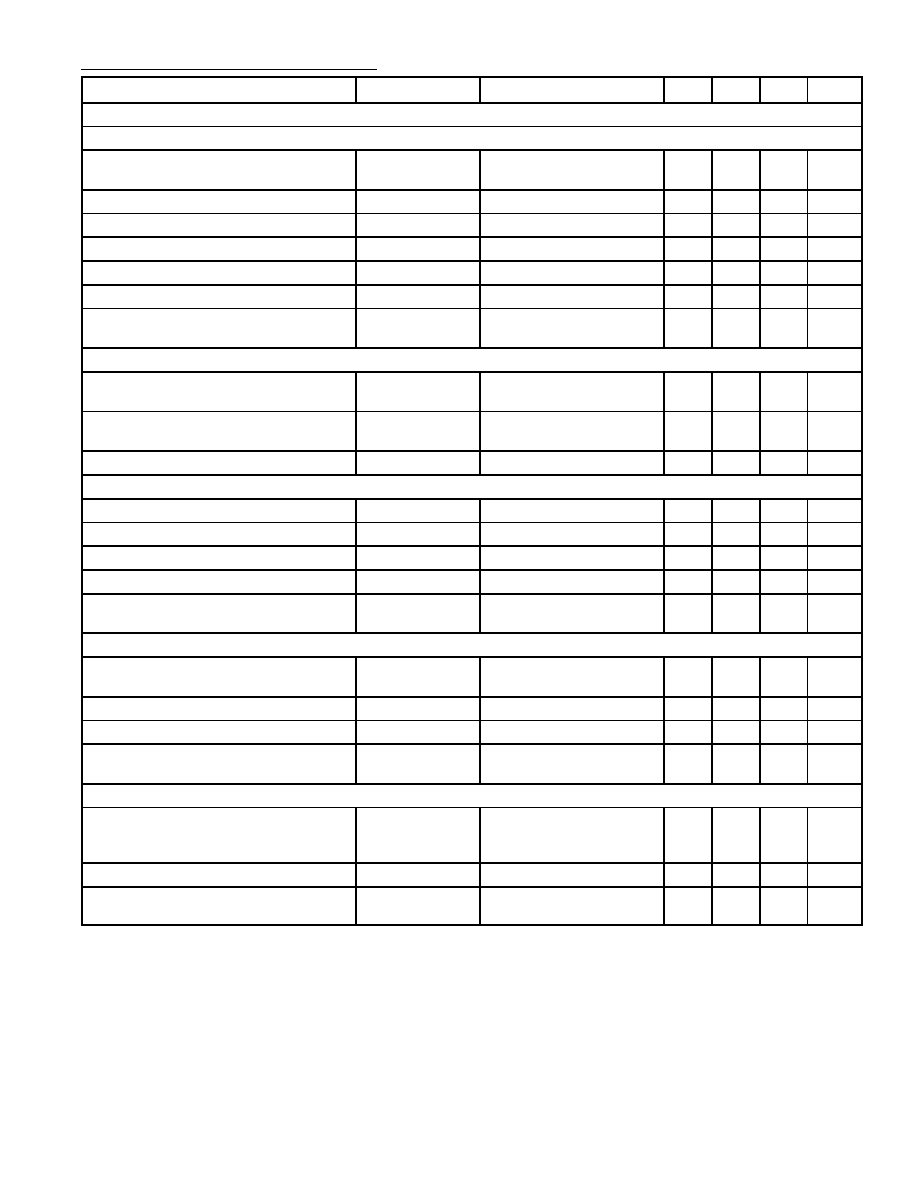
External Cap for Horiz Oscillator
Horiz Size In
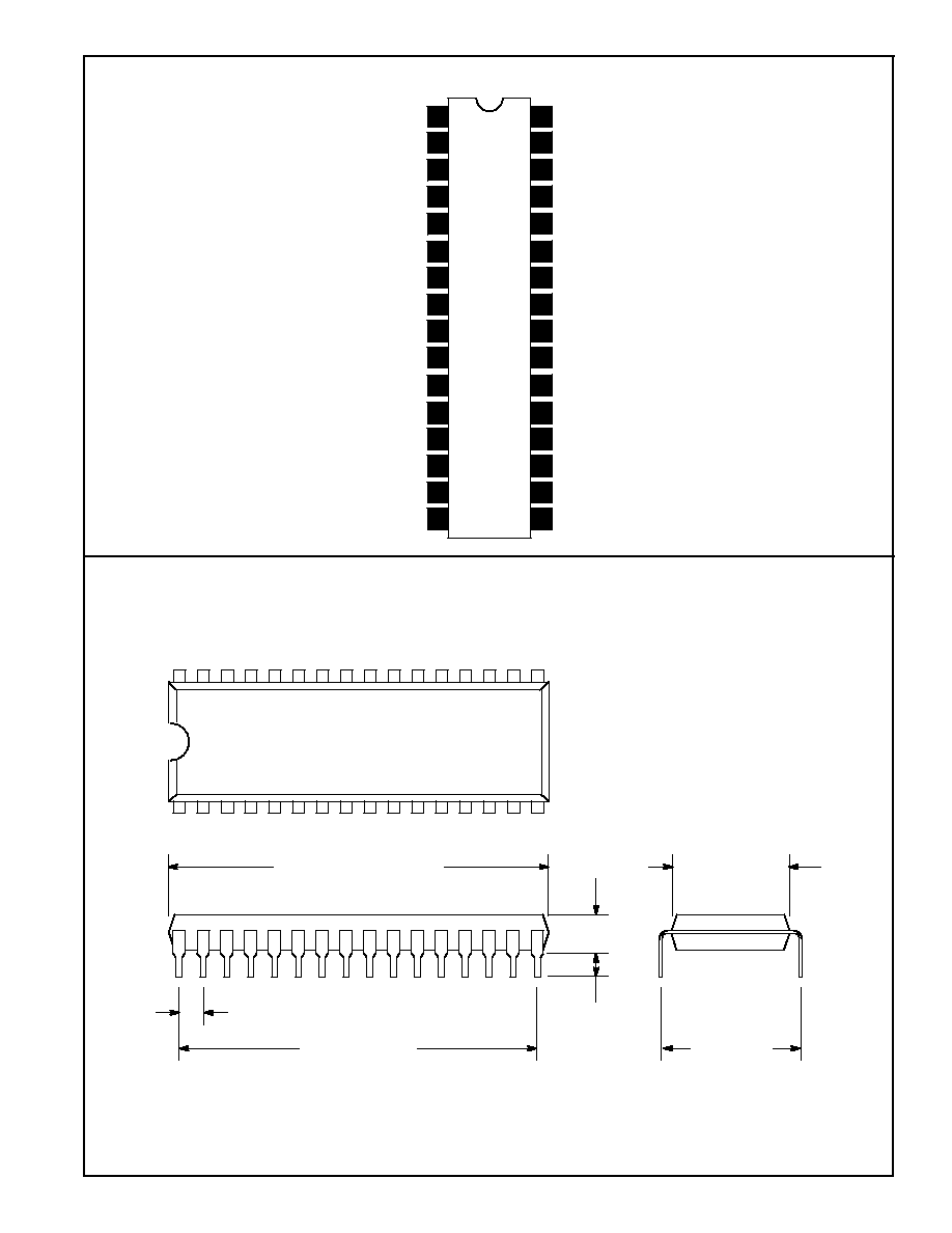
Pin Connection Diagram
External Resistor for Vert Oscillator
External Filter for PLL1
Buffered f/v Voltage Out
Selection In for Horiz Clamping Trigger
B+ Control OTA In
Signal GND
1
2
3
4
Horiz Flyback In
XRay Protection In
B+ Control OTA Out/Comparator In
B+ Control Comparator In/Out
5
6
7
8
32
31
30
29
External Filter for PLL2/Soft Start
Horiz Shift In
28
Reference Current for Horiz Oscillator
27
26
25
External Cap for Vert Oscillator
9
24
10
23
B+ Control Driver Out
Horiz Driver Out
Power GND
Vert Shift In
EW Trapezium Correction In
EW Parabola Amplitude In
Video Clamping Pulse/
EW Parabola Out
Vert SCorrection In
Horiz/Composite Sync In
11
12
13
14
22
External Cap for Vert Amplitude Control
21
20
19
Vert Size In
15
18
16
17
Vert Output 2 (Ascending Sawttoth)
Vert Output 1 (Descending Sawtooth)
Vert Sync Input/Output (TTL Level)
V
CC
(TTL Level or SDyncOnVideo)
Vert Blanking & Protection Out
16
17
1
1.157 (29.4) Max
1.050 (26.7)
.070 ( 1.78)
.185 (4.7)
32
.358 (9.1)
Max
.480
(12.2)
Max
.110
(2.8)
Min