 | –≠–ª–µ–∫—Ç—Ä–æ–Ω–Ω—ã–π –∫–æ–º–ø–æ–Ω–µ–Ω—Ç: NTE7138 | –°–∫–∞—á–∞—Ç—å:  PDF PDF  ZIP ZIP |

NTE7138
Integrated Circuit
Advanced Monitor Video Controller for OSD
Description:
The NTE7138 is an RGB pre≠amplifier in a 20≠Lead DIP type package designed for color monitor
systems with super VGA performance. It is intended for DC or AC coupling of the color signals to the
cathodes of a CRT.
Features:
D
85MHz Video Controller
D
Fully DC Controllable
D
3 Separate Video Channels
D
Input Black Level Clamping
D
White Level Adjustment for 2 Channels Only
D
Brightness Control with Correct Grey Scale Tracking
D
Contrast Control for All 3 Channels Simultaneously
D
Cathode Feedback to Internal Reference for Cut≠Off Control, Which Allows Unstabilized Video
Supply Voltage
D
Current Outputs for RGB Signal Currents
D
RGB Voltage Outputs to External Peaking Circuits
D
Blanking and Switch≠Off Input for Screen Protection
D
Sync On Green Operation Possible
D
On Screen Display (OSD) Facility
Absolute Maximum Ratings:
Supply Voltage (Pin7), V
P
0 to +8.8V
. . . . . . . . . . . . . . . . . . . . . . . . . . . . . . . . . . . . . . . . . . . . . . . . . . . . .
Input Voltage Range (Pin2, Pin5, Pin8), V
i
≠0.1 to V
P
. . . . . . . . . . . . . . . . . . . . . . . . . . . . . . . . . . . . . . .
External DC Voltage Ranges, V
ext
Pin20, Pin17, Pin14
≠0.1 to V
P
. . . . . . . . . . . . . . . . . . . . . . . . . . . . . . . . . . . . . . . . . . . . . . . . . . . .
Pin12, Pin15, Pin18
≠0.1 to +0.7V
. . . . . . . . . . . . . . . . . . . . . . . . . . . . . . . . . . . . . . . . . . . . . . . . .
Pin1, Pin3, Pin6, Pin11
≠0.1 to V
P
. . . . . . . . . . . . . . . . . . . . . . . . . . . . . . . . . . . . . . . . . . . . . . . . . .
Pin9
≠0.1 to V
P
+0.7V
. . . . . . . . . . . . . . . . . . . . . . . . . . . . . . . . . . . . . . . . . . . . . . . . . . . . . . . . . . . . .
Pin10
≠0.1 to V
P
+0.7V
. . . . . . . . . . . . . . . . . . . . . . . . . . . . . . . . . . . . . . . . . . . . . . . . . . . . . . . . . . . .
Average Output Current (Pin14, Pin17, Pin20, Note 1), I
o(av)
0 to 50mA
. . . . . . . . . . . . . . . . . . . . . . .
Peak Output Current (Pin14, Pin17, Pin20), I
OM
0 to 100mA
. . . . . . . . . . . . . . . . . . . . . . . . . . . . . . . . .
Total Power Dissipation, P
tot
1200mW
. . . . . . . . . . . . . . . . . . . . . . . . . . . . . . . . . . . . . . . . . . . . . . . . . . . .
Electrostatic Handling for All Pins (Note 2), V
esd
±
500V
. . . . . . . . . . . . . . . . . . . . . . . . . . . . . . . . . . . . . .
Operating Junction Temperature Range, T
J
≠25
∞
to +150
∞
C
. . . . . . . . . . . . . . . . . . . . . . . . . . . . . . . . . .
Operating Ambient Temperatrure Range, T
A
0
∞
to +70
∞
C
. . . . . . . . . . . . . . . . . . . . . . . . . . . . . . . . . . . .
Storage Temperature Range, T
stg
≠25
∞
to +150
∞
C
. . . . . . . . . . . . . . . . . . . . . . . . . . . . . . . . . . . . . . . . . .
Thermal Resistance, Junction≠to≠Ambient (In Free Air), R
thJA
65K/W
. . . . . . . . . . . . . . . . . . . . . . . .
Note 1. Signal amplitude of 50mA black≠to≠white is possible if the average current (including blank-
ing times and signal variation against time) does not exceed 50mA. The maximum power
dissipation of 1200mW has to be considered.
Note 2. Equivalent to discharging a 200pF capacitor through a 0
series resistor.
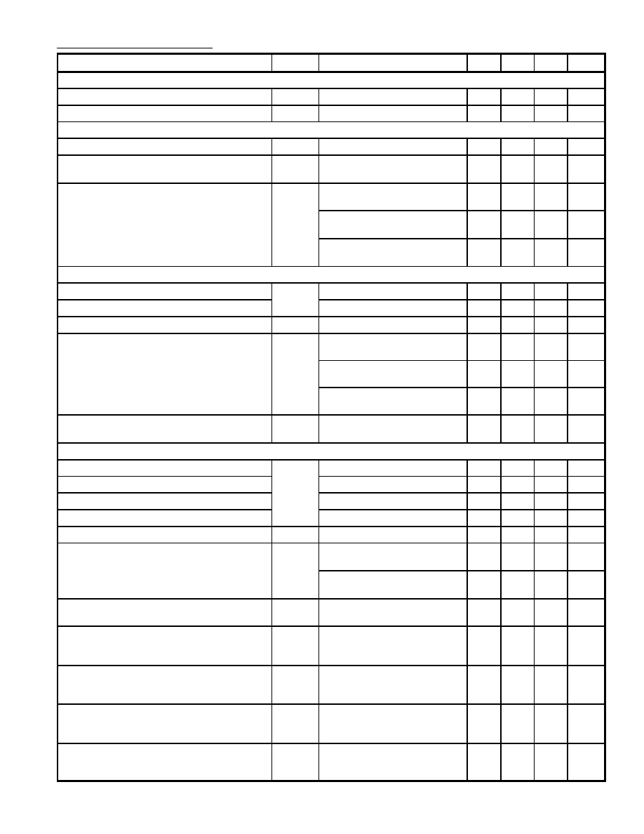
Electrical Characteristics: (V
P
= 8V, T
A
= +25
∞
C, Note 3, Note 4 unless otherwise specified)
Parameter
Symbol
Test Conditions
Min
Typ
Max
Unit
Supply
Supply Voltage Range
V
P
7.2
8.0
8.8
V
Supply Current
I
P
36
48
60
mA
Video Signal Inputs (Channels 1, 2 and 3)
Input Voltage (Black≠to≠White)
V
i(b≠w)
≠
0.7
1.0
V
DC Voltage During Input Clamping
(Artificial Black + V
BE
)
V
l(clamp)
2.8
3.1
3.4
V
DC Input Current
I
I
No Clamping, V
i
= V
l(clamp)
,
T
A
= ≠20
∞
to +70
∞
C
≠0.05 +0.05 +0.25
µ
A
During Clamping,
V
i
= V
l(clamp)
+0.7V
50
75
120
µ
A
During Clamping,
V
i
= V
l(clamp)
≠0.7V
≠120
≠75
≠50
µ
A
Brightness Control (Note 5)
Input Voltage Range
V
i(BC)
1.0
≠
6.0
V
Input Voltage for Nominal Brightness
Pin1 Open≠Circuit
2.0
2.25
2.5
V
Input Resistance
R
i(BC)
40
50
60
k
Black Level Voltage Change at Voltage
Outputs Referred to Reference Black
V
bl
V
i(BC)
= 1.0V
≠13
≠11
≠9.5
%
Level During Output Clamping
(V
i(HBL)
> 1.6V) Related to Output
V
i(BC)
= 6.0V
30
34
37
%
Signal Amplitude with Nominal 0.7V
(P≠P)
Input Signal and Nominal Contrast
(V
i(CC)
= 4.3V) for Any Gain Setting
Pin1 Open≠Circuit
≠
≠
0.8
%
Difference of
V
bl
Between and Two
Channels
V
BT
≠1.2
0
+1.2
%
Contrast Control (Note 6)
Input Voltage Range
V
i(CC)
1.0
≠
6.0
V
Maximum Input Voltage
≠
≠
V
P
≠1
V
Input Voltage Range for Nominal Contrast
Note 7
≠
4.3
≠
V
Input Voltage Range for Minimum Contrast
Pin3 and Pin11 Open≠Circuit
≠
0.7
≠
V
Input Current
I
i(CC)
V
i(CC)
= 4.3V
≠5
≠1
≠0.1
µ
A
Contrast Relative to Nominal Contrast
C/C
nom
V
i(CC)
= 6V, Pin3 and Pin11
Open≠Circuit
2.4
3.4
≠
dB
V
i(CC)
= 1V, Pin3 and Pin11
Open≠Circuit
≠26
≠22
≠19
dB
Tracking of Output Signals of
Channels 1, 2 &3
G
track
1V < V
i(CC)
< 6V, Note 8
≠
0
0.5
dB
Delay Between Leading (Falling) Edges of
Contrast Voltage and Voltage Output
Waveforms
t
df(C)
V
i(CC)
= 4.3V to 0.7V, Input
Fall Time at Pin6: t
f(CC)
= 2ns,
Note 9
≠
7
20
ns
Delay Between Trailing (Rising) Edges of
Contrast Voltage and Voltage Output
Waveforms
t
dr(C)
V
i(CC)
= 0.7V to 4.3V, Input
Rise Time at Pin6: t
f(CC)
= 2ns,
Note 9
≠
15
25
ns
Fall Time of Voltage Output Waveform
t
f(C)
90% to 10% Amplitude, Input
Fall Time at Pin6: t
f(CC)
= 2ns,
Note 9
≠
6
15
ns
Rise Time of Voltage Output Waveform
t
r(C)
10% to 90% Amplitude, Input
Rise Time at Pin6: t
f(CC)
= 2ns,
Note 9
≠
6
15
ns

Electrical Characteristics (Cont'd): (V
P
= 8V, T
A
= +25
∞
C, Note 3, Note 4 unless otherwise specified)
Parameter
Symbol
Test Conditions
Min
Typ
Max
Unit
Gain Control (Channel 1 and Channel 3, Note 10)
Input Voltage
V
i(GC)
1.0
≠
6.0
V
Input Voltage for Nominal Gain
Pin3, Pin11 Open Circuit
3.6
3.75
3.95
V
Input Resistance
R
i(GC)
44
55
66
k
Gain Control Difference Relative to
G
V
i(CC)
= 4.3V, V
i(GC)
= 6V
2.0
2.6
3.3
dB
Nominal Gain (Channels 1 and 3 Only)
V
i(CC)
= 4.3V, V
i(GC)
= 1V
≠5.5
≠5.0
≠4.5
dB
Feedback Input (Channels 1, 2 and 3, Note 11)
Internal Reference Voltage
V
ref(int)
5.6
5.8
6.1
V
Maximum Output Current
I
o(FB)
During Output Clamping,
V
i(FB)
= 3V
≠500
≠100
≠60
nA
Black≠Level Variation at CRT
V
bl(CRT)
Note 12
0
40
200
mV
Variation of V
ref(int)
in the Temperature
Range
V
ref(T)
T
A
= ≠20
∞
to +70
∞
C
0
20
50
mV
Variation of V
ref(int)
with Supply Voltage
V
ref(int)(VP)
7.2V
V
P
8.8V
0
60
100
mV
Voltage Outputs (Channels 1, 2 and 3)
Nominal Signal Output Voltage
(Black≠to≠White Value)
V
o(b≠w)
Pin3 and Pin11 Open≠Circuit,
V
i(CC)
= 4.3V, V
i(b≠w)
= 0.7V
0.69
0.79
0.89
V
Maximum Adjustable Black≠Level Voltage
V
blx(max)
During Output Clamping,
T
A
= ≠20
∞
to +70
∞
C
1.0
1.2
1.4
V
Black≠Level Voltage During Switch≠Off,
Equal to Minimum Adjustable
Black≠Level Voltage
V
bl(SO)
V
i(HBL)
= V
P
, R
O
= 33
,
T
A
= ≠20
∞
to +70
∞
C
30
45
100
mV
Black≠Level Voltage During Test Mode
V
bl(TST)
V
i(HBL)
= V
P
, V
i(CL)
= V
P
,
Pin1 Open≠Circuit,
V
i
= V
i(clamp)
, Note 13
0.3
0.7
1.2
V
Signal≠to≠Noise Ratio
S/N
Note 14
≠
50
44
dB
Output Thermal Distortion
d
O(th)
I
o(b≠w)
= 50mA, Note 15
≠
0.6
1.0
%
Blacl≠Level Variation Between
Clamping Pulses
V
bl(fl)
Line frequency 30kHz
≠
0.5
4.5
mV
Maximum Offset During Sync Clipping
V
offset(max)
V
l
< V
l(clamp)
, Note 16
0
7
15
mV
Variation of Nominal Output Signal
(Black≠to≠White Value) with
Temperature
V
o(b≠w)(T)
Pin3 and Pin11 Open≠Circuit,
V
i(CC)
= 4.3V, V
i(b≠w)
= 0.7V,
T
A
= ≠20
∞
to +70
∞
C
0
2.5
10
%
Current Outputs (Channels 1, 2 and 3, Note 17)
Output Current (Black≠to≠White Value)
I
o(b≠w)
≠
50
≠
mA
With Peaking
≠
≠
100
mA
Start of HF≠Saturation Voltage of
V
20≠19
,
I
o
= 50mA
≠
≠
2.0
V
Output Transistors
V
17≠16
,
V
14≠13
I
o
= 100mA
≠
≠
2.2
V
Output Current During Switch≠Off
I
bl(SO)
V
i(HBL)
= V
P
, R
O
= 33
0
20
900
µ
A
Frequency Response at Voltage Outputs (Note 18)
Gain Decrease by Frequency Response
G
(f)
70MHz, Single Channel
≠
1.3
3.0
dB
Rise Time at Voltage Output
t
r(O)
10% to 90% Amplitude,
Input Rise Time = 1ns
≠
4.1
5.0
ns
Overshoot of Output Signal Pulse Related
to Actual Output Pulse Amplitude
dV
O
Single Channel,
Input Rise Time = 2.5ns,
V
i(b≠w)
= 0.7V, V
i(CC)
= 4.3V,
Pin3 and Pin11 Open≠Circuit
≠
4
8
%

Electrical Characteristics (Cont'd): (V
P
= 8V, T
A
= +25
∞
C, Note 3, Note 4 unless otherwise specified)
Parameter
Symbol
Test Conditions
Min
Typ
Max
Unit
Crosstalk at Voltage Outputs with Speed Up Circuit (Note 18)
Transient Crosstalk
ct(tr)
≠
≠
≠20
dB
Threshold Voltages for Clamping, Blanking and Switch≠Off (Note 19)
Threshold for Horizontal Blanking
(Blanking, Output Clamping)
V
i(HBL)
1.2
1.4
1.6
V
Threshold for Switch≠Off (Blanking,
Minimum Black≠Level, No Output
Clamping)
5.8
6.5
6.8
V
Input Resistance
R
i(HBL)
Against GND
50
80
110
k
Delay Between Horizontal Blanking
Input and Output Signal Blanking
t
d(Hblank)
Input Rise Time at Pin9 > 100ns,
Note 20
≠
40
60
ns
Threshold for Vertical Blanking
(Blanking, No Input Clamping)
V
i(CL)
Note 20
1.2
1.4
1.6
V
Threshold for Vertical Blanking
(Input Clamping, No Blanking)
2.6
3.0
3.5
V
Threshold for Test Mode
(No Clamping, No Blanking
See V
bl(TST)
Above)
For Test Mode Also,
V
i(HBL)
> 6.8V (Switch≠Off)
V
P
≠1
≠
V
P
V
Current
I
i(CL)
V
i(CL)
< V
P
≠1V
≠3
≠1
≠
µ
A
V
i(CL)
V
P
≠1V
µ
A
Rise and Fall Time for Clamping Pulse
t
r(CL)
, t
f(CL)
Note 20
≠
≠
75
ns/V
Width of Clamping Pulse
t
w(clamp)
0.6
≠
≠
µ
s
Delay Between Vertical Blanking Input
and Internal Blanking
t
d(Vblank)
Note 20
260
320
380
ns
Notes to the Characteristics:
Note 3. All voltages measured to GND (Pin4).
Note 4. Definition of levels:
a) Artificial black level: internal signal level behind input emitter follower during input
clamping and signal clipping. This level is inserted instead of the input signal during
blanking.
b) Reference black level: DC voltage during output clamping at voltage outputs, not
influenced by brightness, contrast or gain setting, adjustable by cut≠off stabilization.
c) Cut≠off level: corresponding DC voltage at CRT cathode in closed feedback loop.
d) Black level: actual signal black level at either the voltage outputs or cathode, it can
be adjusted by (brightness x gain), it refers to reference black level or cut≠off level.
e) Ultra≠black level, switch≠off level: lowest adjustable reference black level, lowest
signal level at voltage outputs.
f) The minimum guaranteed control range for reference black level is 0.1 to 1.0V. The
ultra≠black level is dependent on the external resistor R
O
at Pin13, Pin16 and Pin19
(voltage outputs) to GND.
g) V
bl(SO)
x 4.65V
R
o
3.5k
+ R
o
Note 5. Linear control range is 1 to 6V for V
i(BC)
, independent of supply voltage.
Note 6. Linear control range is 1 to 6V vor V
i(BC)
, independent of supply voltage. Open Pin6 leads
to maximum contrast setting. It is recommended not to exceed V
i(CC)
= V
P
≠ 1V to avoid satu-
ration of internal circuitry. For V
i(CC)
< V
i(CC)
0.7V a small negative signal (
≠40dB) will
appear. For frequency dependency of contrast control, see Note 18.
Note 7. Definition for nominal output signals: input V
i(b≠w)
= 0.7V, gain Pin3 and Pin11 open≠circuit,
contrast control V
i(CC)
= V
i(CC)(nom)
.

Notes to the Characteristics (Cont'd):
Note 8.
G
track
= 20 x maximum of
A
30
A
3
dB
A
1
A
10
x
A
20
A
2
log
;
A
1
A
10
x
A
30
A
3
log
;
A
2
A
20
x
log
A
x
: signal output amplitude in channel x at any contrast sertting between 1 and 6V.
A
x0
: signal output amplitude in channel x at nominal contrast and same gain setting.
Note 9. Typical step in contrast voltage and response at signal outputs for nominal input signal
V
i(b≠w)
= 0.7V (OSD fast blanking input/output).
Note10. Linear control range is 1 to 6V for V
i(GC)
, independent of supply voltage.
Note 11. The internal reference voltage can be measured at Pin18, Pin15 and Pin12 (channel feed-
back inputs) during output clamping (V
i(HBL)
= 2V) in closed feedback loop.
Note12. Slow variations of video supply V
CRT
will be suppressed at CRT cathode by cut≠off stabiliza-
tion. Change of V
CRT
by 5V leads to specified cghange of cut≠off voltage.
Note13. The test mode allows testing without input and output clamping pulses. The signal inputs
have to be biased via resistors to the previously measured clamp voltages of approximately
3V (artificial black level + V
BE
). Signal and brightness blanking is not possible during test
mode. The current outputs should be adjusted by resistors >> R
0
from voltage outputs to a
positive voltage (e.g. V
P
).
Note14. The signal≠to≠noise ratio is calculated by the formula (frequency range 1 to 70MHz):
= 20 x log
peak≠to≠peak value of the nominal signal output voltage
RMS value of the noise output voltage
S
N
dB
Note15. Large output swing e.g. I
o(b≠w)
= 50mA leads to signal≠dependent power dissipation in output
transistors. Thermal V
BE
variation is compensated.
Note16. Composite signals will not disturb normal operation because an internal clipping circuit cuts
all signal parts below black level.
Note17. The output current approximately follows the equation I
o
= V
o
1
R
O
+
1
2.2k
≠500
µ
A for
V
o
> V
b(SO)
and with R
O
= external resistor at voltage output to GND. The external RC com-
bination at Pin19, Pin16 and Pin13 (voltage outputs) enables peak currents during tran-
sients.
Note18. Frequency responses, crosstalk aznd pulse response have been measured at voltage out-
puts on a special printed≠circuit board with 50
line in/out connections and without peaking.
Note19. Crosstalk between any two voltage outputs (e.g. channels 1 and 2).
a) Input conditions: one channel (channel1 ) with nominal input signal and minimum
rise time. The inputs of the other channels capacitively coupled to GND (channels 2
and 3). Gain Pin3 and Pin11 open≠circuit.
b) Output conditions: output signal of channel 1 is set by contrast control voltage, to
V
o(b≠w)
= V
o(VOUT1)
= 0.7V, the rise time should be 5ns. Output signal of channel 2 then
is V
o(b≠w)
= V
o(VOUT2)
.
c) Transient crosstalk:
ct(tr)
= 20 x log
V
o(VOUT2)
V
o(VOUT1)
db
d) Crosstalk as a function of frequency has been measured without peaking circuit, with
nominal input signal and nominla settings.
Note20. The internal threshold voltages are derived from a stabilized voltage. The internal pulses are
generated while the input pulses are higher than the thresholds. Voltages less than ≠0.1V
at Pin9 and Pin10 can influence black≠level control and should be avoided.
Note21. The delay between HBL input pulse (horizontakl blanking) and output signal blanking pulse
and also brightness blanking (
V
bl
), at the voltage outputs, depends on the input rise time
of the HBL pulse. The specified values for t
d(Hblank)
are valid for HBL rise times greater than
100ns only.
Note22. For 75ns/V < t
f(CL)
< 240ns/V, generation of internal input clamping and blanking pulse is not
defined. Pulses not exceeding the threshold of input clamping (typical 3V) will be detected
as blanking pulses.

Functional Description:
General
The RGB input signals 0.7V
(P≠P)
are capacitively coupled into the NTE7138 from a low ohmic source
and are clamped to an internal DC voltage (artificial black level). Composite signals will not disturb
normal operations because an internal clipping circuit cuts all signal parts below black level. Channels
1 and 3 have a maximum total voltage gain of 7dB (maximum contrast and maximum individual chan-
nel gain), channel 2 having 4.4dB (maximum contrast and nominal gain). With the nominal channel
gain of 1dB and nominal contrast setting the nominal balck≠to≠white output signal is 0.79V
(P≠P)
.
Brightness, contrast and gain control is by DC voltage.
Brightness Control
Brightness control yeilds a simultaneous signal black≠level shift of the three channels relative to a
reference black level.
For normal brightness (Pin1 open≠circuit) the signal black≠level is equal to the reference black level.
Contrast Control
Contrast is voltage controlled to affect the three channels simultaneously. To provide the correct white
point, individual gain controls adjust the signals of channels 1 and 3 relative to the reference channels
2. Gain setting also changes contrast to achieve correct grey scale tracking.
Output Stages
The output stages provide both voltage and current outputs. External cascode transistors reduce
power consumption of the IC and prevent breakdown of the output transistors. Signal output currents
and peaking characteristics are determined by external components at the voltage outputs and the
video supply. The channels have separate internal feedback loops which ensure large signal linearity
and marginal signal distortion irrespective of output transistor thermal V
BE
variation.
Input Clamping
The clamping pulse is for input clamping only. The input signals are at black level during the clamping
pulse and are clamped to an internal artificial black level. The coupling capacitors provide black≠level
storage. The threshold for the clamping pulse is higher than that for vertical blanking, thereofre, the
rise and fall times of the clamping pulse need to be faster than 75ns/V during transition from 1 to 3.5V.
Vertical Blanking
The vertical blanking pulse will be detected if the input voltage is higher than the threshold voltage
for approximately 320ns but does not exceed the threshold for the clamping pulse in the time between.
During the vertical blanking pulse the input clamping is disabled to avoid misclamping in the event
of composite input signals. The input signal is blanked and the artificial black level is inserted instead.
Also the brightness is set internally to its nominal value, thus the output signal is at reference balck
level. The DC value of the reference black level will be adjusted by cut≠off stabilization.
Horizontal Blanking
During horizontal blanking the output signal is set to reference black level and output clamping is acti-
vated. If the voltage exceeds the switch≠off threshold, the signal is blanked and switched to ultra≠
black level for screen protection and spot suppression during V≠flyback.
Ultra≠black level is the lowest possible channel output voltage and is not dependent on cut≠off stabilization.
Cut≠Off and Black≠Level Stabilization
For cut≠off stabilization (DC coupling to the CRT) and black≠level stabilization (AC coupling) the video
signal at the cathode or the coupling capacitor is divided by an adjustable voltage divider and fed to
the channel feedback inputs. During horizontal blanking time this signal is compared with an internal
DC voltage of approximately 5.8V. Any difference will lead to a reference black≠level correction by
charging or discharging the integrated capacitor which stores the reference black≠level information
between the horizontal blanking pulses.
On Screen Display
For OSD, fast switching of control Pin6 to less than 1V (e.g. 0.7V) blanks the input signals. The OSD
signals can easily be inserted to the external cascode transistor.
Functional Description (Cont'd):
Test Mode
During test mode (Pin9 and Pin10 connected to V
P
) the black levels at the channel voltage outputs
are set internally to typical 0.7V with nominal brightness and 3V DC at channel signal inputs.
Current Output Ch2
Current Output Ch1
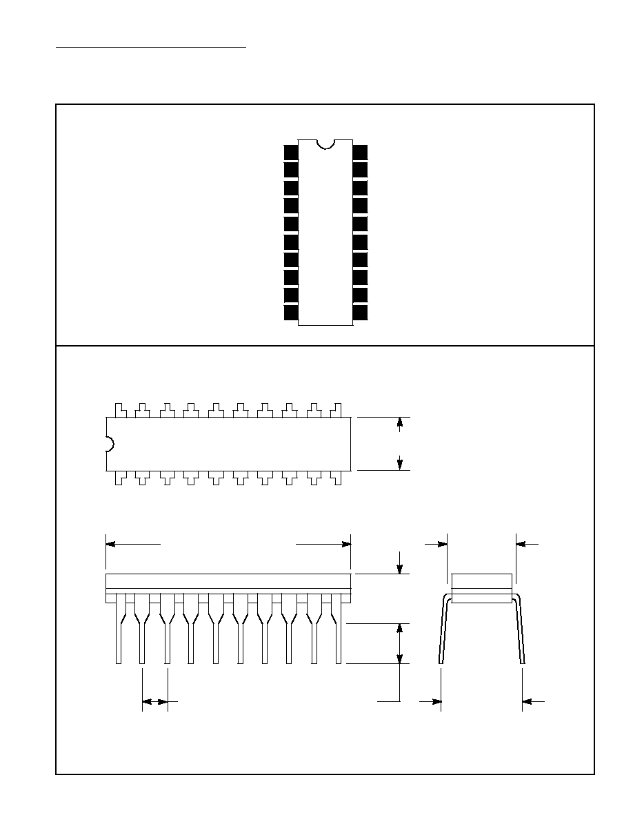
Pin Connection Diagram
Gain Control Ch3
Feedback Ch2
Input Clamping, Vertical Blanking,
Signal Input Ch2
Voltage Output Ch3
Horizontal Blanking, Swith Off
1
2
3
4
Brightness Control
Signal Input Ch1
Gain Control Ch1
GND
5
6
7
8
20
19
18
17
Voltage Output Ch1
Feedback Ch1
16
Voltage Output Ch2
15
14
13
Feedback Ch3
9
12
10
11
Contrast Control, OSD Swithc
Signal Input Ch3
.995 (25.3) Max
.280 (7.12) Max
.100 (2.54)
.125 (3.17) Min
.385 (9.8)
.300 (7.62)
.280
(7.1)
1
10
20
11
V
P
Current Output Ch3
Test Mode