
NTE7141
Integrated Circuit
Dual BIMOS Operational Amplifier
w
/MOSFET Input, Bipolar Output
Description:
The NTE7141 is a dual, operational amplifier in an 8≠Lead Mini≠DIP type package that combines the
advantages of MOS and bipolar transistors on the same monolithic chip. The gate≠protected MOS-
FET (PMOS) input transistors provide high input impredance and a wide common≠mode input volt-
age range (typically to 0.5V below the negative supply rail). The bipolar output transistors allow a wide
output voltage swing and provide a high output current capability.
Features:
D
Internally Compensated
D
MOSFET Input Stage:
Very High Input Impedance
Very Low Input Current
Wide Common≠Mode Input Voltage Range
Rugged Input Stage ≠ Bipolar Diode Protected
D
Directly Replaces Industry Type 1458 in Most Applications
D
Operation From 4V≠to≠36V Single or Dual Supplies
D
Characterized for
±
15V Operation for TTL Supply Systems with Operation down to 4V
D
Wide Bandwidth
D
High Voltage≠Follower Slew Rate
D
Output Swings to Within 0.5V of Negative Supply at V+ = 5V, V≠ = 0
Applications:
D
Ground≠Referenced Single≠Supply Amplifiers in Automobile and Portable Instrumentation
D
Sample and Hold Amplifiers
D
Long≠Duration Timers/Multivibrators (Microseconds ≠ Minutes ≠ Hours)
D
Photocurrent Instrumentation
D
Active Filters
D
Intrusion Alarm Systems
D
Comparators
D
Instrumentation Amplifiers
D
Function Generators
D
Power Supplies

Absolute Maximum Ratings:
DC Supply Voltage (Between V+ and V≠ Terminals)
36V
. . . . . . . . . . . . . . . . . . . . . . . . . . . . . . . . . . . .
Operating Voltage Range
4 to 36V or
±
2 to
±
18V
. . . . . . . . . . . . . . . . . . . . . . . . . . . . . . . . . . . . . . . . . .
Differential≠Mode Input Voltage
±
8V
. . . . . . . . . . . . . . . . . . . . . . . . . . . . . . . . . . . . . . . . . . . . . . . . . . . . . .
Common≠Mode DC Input Voltage
(V+ +8V) to (V≠ ≠0.5V)
. . . . . . . . . . . . . . . . . . . . . . . . . . . . . . . . . . .
Input≠Terminal Current
1mA
. . . . . . . . . . . . . . . . . . . . . . . . . . . . . . . . . . . . . . . . . . . . . . . . . . . . . . . . . . . . .
Device Dissipation, P
D
630mW
. . . . . . . . . . . . . . . . . . . . . . . . . . . . . . . . . . . . . . . . . . . . . . . . . . . . . . . . . . .
Derate Linearly Above +55
∞
C
6.67mW/
∞
C
. . . . . . . . . . . . . . . . . . . . . . . . . . . . . . . . . . . . . . . . . . .
Operating Temperature Range, T
opr
≠40
∞
to +85
∞
C
. . . . . . . . . . . . . . . . . . . . . . . . . . . . . . . . . . . . . . . . .
Storage Temperature Range, T
stg
≠65
∞
to +150
∞
C
. . . . . . . . . . . . . . . . . . . . . . . . . . . . . . . . . . . . . . . . . .
Lead Temperature (During Soldering, 1/16" from case, 10sec max), T
L
+265
∞
C
. . . . . . . . . . . . . . . . .
Output Short≠Circuit Duration (Note 1)
Unlimited
. . . . . . . . . . . . . . . . . . . . . . . . . . . . . . . . . . . . . . . . . . .
Note 1. Short circuit may be applied to GND or to either supply. Temperature and/or supply voltages
must be limited to keep dissipation within maximum rating.
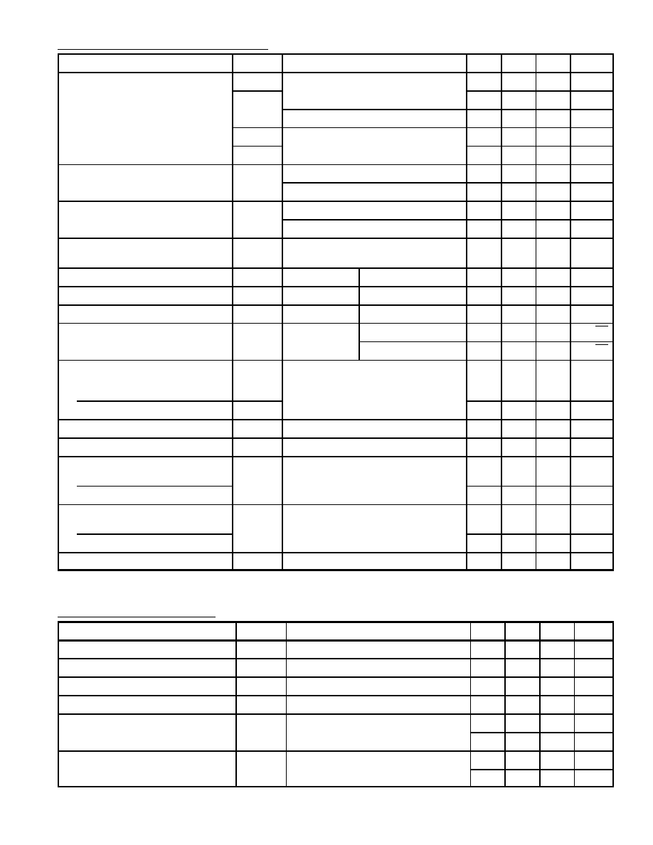
Electrical Characteristics: (V+ = +15V, V≠ = ≠15V unless otherwise specified)
Parameter
Symbol
Test Conditions
Min
Typ
Max
Unit
Input Offset Voltage
|V
IO
|
T
A
= +25
∞
C
≠
5
15
mV
T
A
= ≠40
∞
to +85
∞
C
≠
10
≠
mV
Input Offset Current
|I
IO
|
T
A
= +25
∞
C
≠
0.5
30
pA
T
A
= +85
∞
C
≠
32
≠
pA
Input Current
I
I
T
A
= +25
∞
C
≠
10
50
pA
T
A
= +85
∞
C
≠
640
≠
pA
Large≠Signal Voltage Gain
A
OL
Note 2
T
A
= +25
∞
C
20k
100k
≠
V/V
86
100
≠
dB
T
A
= ≠40
∞
to +85
∞
C
≠
63k
≠
V/V
≠
96
≠
dB
Common≠Mode Rejection Ratio
CMRR
T
A
= +25
∞
C
≠
32
320
µ
V/V
70
90
≠
dB
T
A
= ≠40
∞
to +85
∞
C
≠
32
≠
µ
V/V
≠
90
≠
dB
Common≠Mode Input≠Voltage
Range
V
ICR
T
A
= +25
∞
C
≠15
≠15.5
to
+12.5
+11
V
T
A
= ≠40
∞
to +85
∞
C
≠
≠15
to
+12.3
≠
V
Power Supply Rejection Ratio
V
IO
/
V T
A
= +25
∞
C
≠
100
150
µ
V/V
PSSR
76
80
≠
dB
V
IO
/
V T
A
= ≠40
∞
to +85
∞
C
≠
150
≠
µ
V/V
PSSR
≠
76
≠
dB
Note 2. V
O
= 26V
P≠P
, +12V, ≠14V and R
L
= 2k
.
Electrical Characteristics (Cont'd): (V+ = +15V, V≠ = ≠15V unless otherwise specified)
Parameter
Symbol
Test Conditions
Min
Typ
Max
Unit
Maximum Output Voltage
V
OM
+
T
A
= +25
∞
C, R
L
= 2k
+12
+13
≠
V
V
OM
≠
≠14
≠14.4
≠
V
T
A
= +25
∞
C, Note 3
0.4
0.13
≠
V
V
OM
+
T
A
= ≠40
∞
to +85
∞
C, R
L
= 2k
≠
+12.4
≠
V
V
OM
≠
≠
≠14.2
≠
V
Supply Current, For Both Amps
I+
T
A
= +25
∞
C
≠
8
12
mA
T
A
= ≠40
∞
to +85
∞
C
≠
8.4
≠
mA
Total Device Dissipation
P
D
T
A
= +25
∞
C
≠
240
360
mW
T
A
= ≠40
∞
to +85
∞
C
≠
252
≠
mW
Temperature Coefficient of
Input Offset Voltage
V
IO
/
T
T
A
= ≠40
∞
to +85
∞
C
≠
15
≠
µ
A/
∞
C
Input Resistance
R
I
T
A
= +25
∞
C
≠
1.5
≠
T
Input Capacitance
C
I
T
A
= +25
∞
C
≠
4
≠
pF
Output Resistance
R
O
T
A
= +25
∞
C
≠
60
≠
Equivalent Wideband Input Noise
e
n
T
A
= +25
∞
C,
f = 1kHz
≠
40
≠
nV/
Hz
Voltage
R
S
= 100
f = 10kHz
≠
12
≠
nV/
Hz
Short≠Circuit Current to Opposite
Supply
Source
I
OM
+
T
A
= +25
∞
C
≠
40
mA
Sink
I
OM
≠
≠
11
≠
mA
Gain≠Bandwidth Product
f
T
T
A
= +25
∞
C
≠
4.5
≠
MHz
Slew Rate
SR
T
A
= +25
∞
C
≠
9
≠
V/
µ
s
Transient Response:
Rise Time
t
r
T
A
= +25
∞
C, R
L
= 2k
, C
L
= 100pF
≠
0.08
≠
µ
s
Overshoot
≠
10
≠
%
Setting Time at 10V
P≠P
1mV
t
s
T
A
= +25
∞
C, R
L
= 2k
, C
L
= 100pF,
≠
4.5
≠
µ
s
10mV
Voltage Follower
≠
1.4
≠
µ
s
Crosstalk
CT
T
A
= +25
∞
C, f = 1kHz
≠
120
≠
dB
Note 3. V+ = 5V, V≠ = GND, I
Sink
= 200
µ
A.
Electrical Characteristics: (T
A
= +25
∞
C, V+ = +5V, V≠ = ≠5V unless otherwise specified)
Parameter
Symbol
Test Conditions
Min
Typ
Max
Unit
Input Offset Voltage
|V
IO
|
≠
5
≠
mV
Input Offset Current
|I
IO
|
≠
0.1
≠
pA
Input Current
I
I
≠
2
≠
pA
Input Resistance
R
I
≠
1
≠
T
Large≠Signal Voltage Gain
A
OL
≠
100k
≠
V/V
≠
100
≠
dB
Common≠Mode Rejection Ratio
CMRR
≠
32
320
µ
V/V
70
90
≠
dB
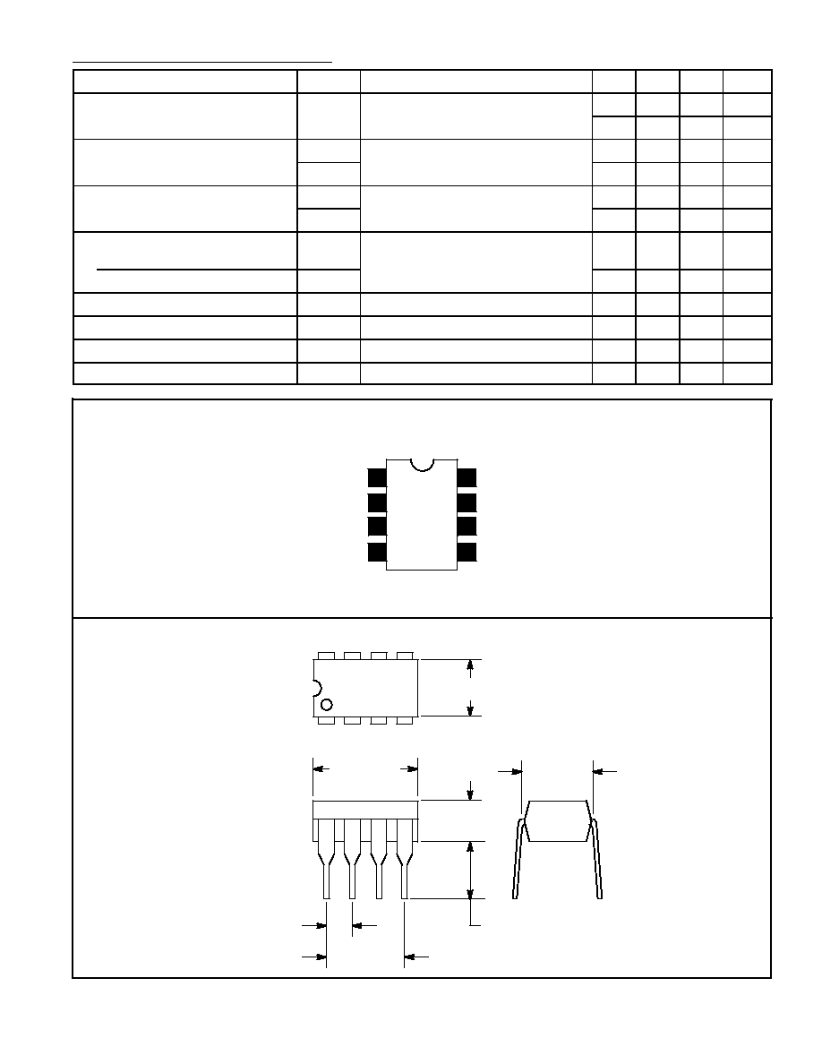
Electrical Characteristics (Cont'd): (T
A
= +25
∞
C, V+ = +5V, V≠ = ≠5V unless otherwise specified)
Parameter
Symbol
Test Conditions
Min
Typ
Max
Unit
Common≠Mode Input≠Voltage Range
V
ICR
≠
≠0.5
≠
V
≠
+2.6
≠
V
Power Supply Rejection Ratio
V
IO
/
V
≠
31.6
≠
µ
V/V
PSSR
≠
90
≠
dB
Maximum Output Voltage
V
OM
+
≠
3.0
≠
V
V
OM
≠
≠
0.3
≠
V
Maximum Output Current:
Source
I
OM
+
≠
20
≠
mA
Sink
I
OM
≠
≠
1
≠
mA
Slew Rate
SR
≠
7
≠
V/
µ
s
Gain≠Bandwidth Product
f
T
≠
4.5
≠
MHz
Supply Current
I+
≠
4
≠
mA
Device Dissipation
P
D
≠
20
≠
mW
Pin Connection Diagram
1
4
.260 (6.6)
.390 (9.9)
Max
8
5
.155
(3.93)
.145 (3.68)
.300
(7.62)
.300 (7.62)
.100 (2.54)
V+
1
2
3
4
Output A
Invert Input A
Non≠Invert Input A
V≠
8
7
6
5
Output B
Invert Input B
Non≠Invert Input B