 | –≠–ª–µ–∫—Ç—Ä–æ–Ω–Ω—ã–π –∫–æ–º–ø–æ–Ω–µ–Ω—Ç: NTE7151 | –°–∫–∞—á–∞—Ç—å:  PDF PDF  ZIP ZIP |

NTE7151
Integrated Circuit
I
2
C Bus Control NTSC 1≠Chip Color TV IC
Description:
The NTE7151 is an integrated circuit in a 56≠Lead DIP type package designed for use as a PIF, SIF,
video, chroma and deflection circuit for NTSC color TVs. This device also provides audio/video
switching and a text interface.
Features:
PIF Circuit
D
PLL Type IF Demodulation (Bus Alignment)
D
Adjustment Free AFT Without Tank Coil
D
RF AGC Output (Delay Point: Bus Alignment)
D
Dual Time Constant Fast AGC
Video Circuit
D
Black Stretcher
D
DC Restoration Circuit
D
D.L. Aperture Compensate Circuit (Bus Control)
D
Uni≠Color Circuit (Bus Control)
D
3.58MHz Trap Filter Circuit (Bus ON/OFF)
D
Y Delay Line Circuit
D
Internal Filter Auto≠Adjust Circuit (F
SC
Link Type)
Chroma Circuit
D
Color Control Circuit (Bus Control)
D
Tint Control Circuit (Bus Control)
D
B.P.F. / T.O.F. Circuit (Bus Select)
D
Included ACC/Killer Filter
SIF Circuit
D
Inter Carrier SIF System
D
External Sound Select Switch (Bus Select)
D
Attenuator Circuit (Bus Control)
Text Circuit
D
Linear RGB Input
D
Cut Off/Drive Adjustment (Bus Adjustment)
D
RGB Primary Color Output
Deflection Circuit
D
Adjustment Free Countdown System
D
Sync. Separation Output
D
X≠Ray Protect Circuit
D
Vertical Amplitude Adjustment (Bus Adjustment)
D
Vertical Ramp Output
D
Dual Time Constant AFC Circuit
D
Auto≠Slicer Type High Performance Sync. Separation Circuit
D
Horizontal and Vertical Position Adjustment (Bus Adjustment)

Absolute Maximum Ratings: (T
A
= +25
∞
C unless otherwise specified)
Power Supply Voltage, V
CC
12V
. . . . . . . . . . . . . . . . . . . . . . . . . . . . . . . . . . . . . . . . . . . . . . . . . . . . . . . . . .
Power Dissipation, P
D
max
2.19W
. . . . . . . . . . . . . . . . . . . . . . . . . . . . . . . . . . . . . . . . . . . . . . . . . . . . . . . . .
Derate Above 25
∞
C
17.5mW/
∞
C
. . . . . . . . . . . . . . . . . . . . . . . . . . . . . . . . . . . . . . . . . . . . . . . . . . . .
Input Terminal Voltage, V
in
GND≠0.3V to V
CC
+0.3V
. . . . . . . . . . . . . . . . . . . . . . . . . . . . . . . . . . . . . . . .
Input Signal Amplitude, e
in
4V
P≠P
. . . . . . . . . . . . . . . . . . . . . . . . . . . . . . . . . . . . . . . . . . . . . . . . . . . . . . . .
Operating Temperature Range, T
opr
≠20
∞
to +65
∞
C
. . . . . . . . . . . . . . . . . . . . . . . . . . . . . . . . . . . . . . . . .
Storage Temperature Range, T
stg
≠55
∞
to +150
∞
C
. . . . . . . . . . . . . . . . . . . . . . . . . . . . . . . . . . . . . . . . . .
Recommended Operating Conditions:
Parameter
Symbol
Test Conditions
Min
Typ
Max
Unit
PIF Power Supply Voltage
V
CCP
8.5
9.0
9.5
V
SIF Power Supply Voltage
V
CCS
8.5
9.0
9.5
V
V/C/D Power Supply Voltage
V
CCV
8.5
9.0
9.5
V
H. V
CC
Power Supply Voltage
H. V
CC
8.5
9.0
9.5
V
D. V
CC
Power Supply Voltage
D. V
CC
2.7
3.3
3.8
V
TV External Video Input Level
V
in37/39
Including Sync.
≠
1.0
≠
V
P≠P
Standard Video Input Level
V
in43
Including Sync.
≠
1.0
≠
V
P≠P
Standard Chroma Input Level
V
in45
At Burst Signal
≠
286
≠
mV
P≠P
FBP Width
T
FBP
V
th
= 1.4V, V
CC
= ≠1.4V
10
12
≠
µ
s
FBP Input Flow In Current
I
FBP
max
≠
≠
2
mA
PIF Output Load Resistor
R
OP
2.0
8.2
≠
k
SIF Output Load Resistor
R
OS
1.0
8.2
≠
k
RGB Output Load Resistor
R
ORGB
≠
1.8
≠
k
Horizontal Output Load Resistor
R
HOUT
maximum 10mA
330
800
≠
Vertical Output Load Resistor
R
VOUT
4.1
5.7
≠
k
Sync.Separation Output Flow In Current
I
sync
max
≠
≠
1
mA
DC Electrical Characteristics: (V
CC
= 9V, H. V
CC
= 9V, T
A
= +25
∞
C unless otherwise specified)
Parameter
Symbol
Test Conditions
Min
Typ
Max
Unit
Sound Output (Pin1)
V
1
3.2
3.7
4.2
V
Sound Output (Pin2)
V
2
3.2
3.7
4.2
V
RF AGC (Pin3)
V
3
≠
0.0
0.5
V
AGC Filter (Pin5)
V
5
7.0
7.5
8.0
V
PIF GND (Pin6)
GND
≠
0.0
≠
V
PIF Input (Pin7)
V
7
1.5
2.0
2.5
V
PIF Input (Pin8)
V
8
≠
0.0
0.5
V
PIF V
CC
(Pin9)
V
CC
≠
9.0
≠
V
Loop Filter (Pin10)
V
10
≠
4.5
≠
V
APC Filter (Pin11)
V
11
6.0
6.5
7.0
V
VCXO (Pin12)
V
12
5.3
5.8
6.3
V
V/C/D GND (Pin13)
GND
≠
0.0
≠
V
F≠BLK (Pin14)
V
14
≠
0.0
≠
V
Analog R Input (Pin15)
V
15
4.4
4.9
5.4
V
Analog G Input (Pin16)
V
16
4.4
4.9
5.4
V
Analog B Input (Pin17)
V
17
4.4
4.9
5.4
V

DC Electrical Characteristics (Cont'd): (V
CC
= 9V, H. V
CC
= 9V, T
A
= +25
∞
C unless otherwise
specified)
Parameter
Symbol
Test Conditions
Min
Typ
Max
Unit
D. V
CC
(Pin18)
V
CC
≠
3.3
≠
V
R Output (Pin19)
V
19
BRT, C.O Cent
2.4
2.7
2.9
V
G Output (Pin20)
V
20
BRT, C.O Cent
2.4
2.7
2.9
V
B Output (Pin21)
V
21
BRT, C.O Cent
2.4
2.7
2.9
V
V SEPA (Pin25)
V
25
5.8
6.3
6.8
V
H. V
CC
(Pin26)
V
26
≠
9.0
≠
V
SCL (Pin27)
V
27
4.5
5.0
5.5
V
SDA (Pin28)
V
28
4.5
5.0
5.5
V
X≠RAY (Pin29)
V
29
≠
0.0
≠
V
H. AFC (Pin33)
V
33
7.0
7.5
8.0
V
32f
H
VCO (Pin34)
V
34
5.5
6.0
6.5
V
D. GND (Pin35)
GND
≠
0.0
≠
V
ABL (Pin36)
V
36
BRT, COL Cent
2.9
3.4
3.9
V
TV Input (Pin37)
V
37
2.9
3.0
3.9
V
ACL (Pin38)
V
38
BRT, COL Cent
2.9
3.4
3.9
V
EXT. Video Input (Pin39)
V
39
1.1
1.6
2.1
V
Black DET (Pin40)
V
40
6.1
6.6
7.1
V
AV/SW Output (Pin41)
V
41
1.8
2.3
2.8
V
DC Rest (Pin42)
V
42
5.5
6.0
6.5
V
Y Input (Pin43)
V
43
4.0
4.5
5.0
V
AFT (Pin44)
V
44
2.0
2.5
3.0
V
Chroma Input (PIn45)
V
45
1.6
1.85
2.1
V
V / C / D V
CC
(Pin46)
V
46
≠
9.0
≠
V
TV DET. Output (Pin47)
V
47
4.7
5.2
5.7
V
SIF V
CC
(Pin48)
V
CC
≠
9.0
≠
V
SIF GND (Pin51)
GND
≠
0.0
≠
V
Limiter Input (Pin52)
V
52
≠
0.0
0.5
V
Audio TV Input (Pin53)
V
53
2.5
3.0
3.5
V
De≠Emphasis (Pin54)
V
54
Pin4 GND
4.0
4.5
5.0
V
EXT. Audio Input (Pin55)
V
55
2.5
3.0
3.5
V
EXT. Audio Input (Pin56)
V
55
2.5
3.0
3.5
V
Current Consumption
IF Power Supply Current
I
cci
32.8
46.0
52.0
mA
V / C / D Power Supply Current
I
ccv
52.7
71.0
76.8
mA
H. V
CC
Power Supply Current
I
cch
10.7
14.0
18.4
mA
D. V
CC
Power Supply Current
I
ccd
5.2
10.0
11.6
mA

AC Electrical Characteristics: (V
CC
= 9V, H. V
CC
= 9V, T
A
= +25
∞
C unless otherwise specified)
Parameter
Symbol
Test Conditions
Min
Typ
Max
Unit
PIF
Video Detected Output Level
V
O1
1.7
2.0
2.3
V
P≠P
V
O2
2.0
2.5
3.0
V
P≠P
Input Sensitivity
V
IN
min
≠
42
≠
dB
µ
V
V
IN
max
100
107
≠
dB
µ
V
Sync Tip Level
V
SYNC
2.6
2.9
3.2
V
Output Level for No Input
V
IF
4.8
5.2
5.6
V
Differential Gain
DG
≠
2
5
%
Differential Phase
DP
≠
2
5
DEG
PIF Output Frequency Characteristics
f
c
5
7
≠
MHz
Carrier Wave Compression Ratio
CR
50
55
≠
dB
2
nd
Harmonics Compression Ratio
HR
50
55
≠
dB
PIF Input Resistance
R
iPIF
≠
1.5
≠
k
PIF Input Capacitance
C
iPIF
≠
3.8
≠
pF
Signal to Noise Ratio
S/N
52
55
≠
dB
920kHz Beat
I
9200
42
45
≠
dB
IF AGC Range
RW
AGC
61
65
69
dB
IF AGC Voltage
V
5MEAN
4.2
4.5
4.8
V
V
5
max
7.4
7.6
≠
V
V
5
min
≠
3.8
≠
V
RF AGC Voltage
V
3
max
7.7
8.2
≠
V
V
3
min
≠
0.0
0.5
V
RF AGC Control Range
D
G
RFAGC
35
40
≠
dB
AFT Center Voltage
V
4CENT
2.2
2.5
2.8
V
AFT Voltage
V
4
max
4.4
4.8
≠
V
V
4
min
≠
0.2
0.5
V
AFT Sensitivity
m
AFT
≠
40
≠
kHz/V
AFT Output Resistance
R
AFTOUT
40
50
60
k
PIF VCO Control Sensitivity
b
IFVCO
2.0
2.5
≠
MHz/V
PIF VCO Pull≠In Range
f
ph
1.0
1.5
≠
MHz
f
pl
1.0
1.5
≠
MHz
PIF VCO Control Range
f
PIFVCO
≠
4.4
≠
MHz
SIF
Sound Output Level
V
AAC
400
500
600
mV
rms
V
ADC
≠
4.5
≠
V
Sound Distortion
V
AUDIO
≠
0.3
1.0
%
AMR
AMR
50
60
≠
dB
Limiting Sensitivity
V
LIM
≠
35
≠
dB
µ
V
Sound Output Frequency Characteristics
f
AUDIOH
≠
130
≠
kHz
f
AUDIOL
≠
≠130
≠
kHz
Sound Output Resistance
R
SOUT
24
30
36
k

AC Electrical Characteristics (Cont'd):
(V
CC
= 9V, H. V
CC
= 9V, T
A
= +25
∞
C unless otherwise
specified)
Parameter
Symbol
Test Conditions
Min
Typ
Max
Unit
ATT
ATT Gain
G
ATTMAXE
≠2.0
0.0
+2.0
dB
G
ATTMAXT
4.0
6.0
8.0
dB
G
ATTMEAN
≠16
≠12
≠9
dB
G
ATTMIN
≠99
≠85
≠
dB
DC Voltage Drift
V
1VAR
≠
≠
50
mV
V
1DC
3.2
3.7
4.2
V
Input Impedance
R
i53
≠
30
≠
k
R
i55
≠
47
≠
k
Balance Characteristics
B
MAX
45
58
70
dB
B
MIN
≠70
≠58
≠45
dB
Video
Input Impedance
R
i41
100
≠
≠
k
Input Dynamic Range
V
di41
1.0
1.2
1.5
V
Video Total Gain
G
Y
4.5
5.0
≠
Video Frequyency Characteristic
f
Y
6.0
7.0
≠
MHz
Maximum Output
V
do1
7.5
8.0
≠
V
Black Expansion Amp Gain
G
BAMP
1.18
1.43
1.68
Black Expansion Start Point
G
BSTP
40
50
60
IRE
DC Restoration
T
DC
100
103
105
%
Sharpness Control Characteristics
G
SHcent
1
4
7
dB
G
SHmax
9
12
15
dB
G
SHmin
≠
≠18
≠15
dB
Sharpness Delay Time
t
SHDLY
≠
125
≠
ns
Contrast Control Characteristics
G
CNcent
4.5
6.0
7.5
dB
G
CNmin
22.5
24.0
28.5
dB
H. V≠BLK Output Voltage
V
BLK
≠
0.7
1.0
V
V≠BLK Width
T
VBLK
3.5 to 24.0
H
f
sc
Trap Gain
G
TRAP
≠
≠28
≠20
dB
OSD
OSD Switching Voltage
V
thOSD
0.7
1.0
1.3
V
OSD Delay Time
t
OSDDLY
≠
15
30
ns
OSD Delay Time Difference
t
OSDD
≠
5
10
ns
OSD Rising Time
t
R
≠
15
30
ns
OSD Falling Time
t
F
≠
15
30
ns
Input Clamp Voltage
V
OSDC
4.4
4.9
5.4
V
OSD Gain
G
OSD
1.8
2.0
2.2
Input Dynamic Range
V
diOSD
2.0
2.2
2.4
V
Cutoff Drive
Brightness Control Characteristics
V
BRTmax
3.6
4.0
4.3
V
V
BRTcen
2.4
2.7
3.0
V
V
BRTmin
1.0
1.4
1.7
V

AC Electrical Characteristics (Cont'd):
(V
CC
= 9V, H. V
CC
= 9V, T
A
= +25
∞
C unless otherwise
specified)
Parameter
Symbol
Test Conditions
Min
Typ
Max
Unit
Cutoff Drive (Cont'd)
Brightness Control Difference Between 3 Axes
VRGB
≠50
0
+50
mV
Cutoff Control Characteristics
V
cutmax
0.5
0.65
0.8
V
V
cutcen
≠
0.0
≠
V
V
cutmin
≠0.8
≠0.65
≠0.5
V
Drive Control Characteristics
G
drvmax
3.75
4.25
4.75
dB
G
drvmin
≠4.0
≠3.5
≠3.0
dB
Chroma
Input Dynamic Range
V
di45
0.95
1.5
1.7
V
ACC Characteristics
e
a
≠23
≠20
≠17
dB
e
b
3
6
9
dB
A
0.9
1.0
1.1
Killer Point
EK
≠48
≠46
≠43
dB
VCXO Frequency Control Range
D
f
VCXO
±
500
±
600
≠
Hz
VCXO Frequency Control Sensitivity
b
VCXO
≠
1.0
≠
Hz/mV
VCXO Pull≠In Range
f
VCXOPL
±
300
±
450
≠
Hz
Demodulate Relative Gain
R/B
0.78
0.83
0.88
G/B
0.31
0.35
0.39
Demodulate Relative Phase
R≠B
84
91
98
DEG
G≠B
233
240
247
DEG
Carrier Wave Remain
E
CR
≠
20
40
mV
P≠P
E
CB
≠
20
40
mV
P≠P
E
CG
≠
20
40
mV
P≠P
Color Control Characteristics
V
CLRmax
3.9
4.1
4.3
V
P≠P
G
CLRcen
4.5
6.0
7.5
dB
G
CLRmin
38
40
≠
dB
Uni≠Color Control Characteristics
G
UNIcen
4.5
6.0
7.5
dB
G
UNImin
22
24
26
dB
Tint Control Characteristics
q
TNTcen
≠7
0
+7
DEG
q
TNT
±
35
±
45
±
55
DEG
Video Chroma Delay Time
t
V≠C
≠30
0
+30
ns
Deflection
Horizontal Free Running Frequency
f
H
≠100
0
+100
Hz
H. Out Pulse Duty
T
H
38
41
44
%
H. Out Voltage
V
HL
≠
0.2
0.3
V
V
HH
2.5
3.0
3.5
V
VCO OSC Start Voltage
V
OSCmin
3.0
3.5
4.0
V
H. Out Start Voltage
V
HST
3.7
4.0
≠
V
H. Frequency Control Range
D
f
H
±
500
±
650
≠
Hz
H. Frequency Control Sensitivity
b
H
≠
500
≠
Hz/V
H. Sync Pull≠In Range
D
f
HPUL
±
450
±
500
≠
Hz
H. Pull≠In Stop Period
T
HSTP
259 to 272
H
AC Electrical Characteristics (Cont'd):
(V
CC
= 9V, H. V
CC
= 9V, T
A
= +25
∞
C unless otherwise
specified)
Parameter
Symbol
Test Conditions
Min
Typ
Max
Unit
Deflection (Cont'd)
AFC≠2 Control Range
T
AFC2
16
17
≠
µ
s
Horizontal Position Adjustment
T
PAFC2
≠
±
3
≠
µ
s
X≠Ray Protection Detection Voltage
V
XDET
3.35
3.5
3.65
V
X≠Ray Protection Hold Voltage
V
XHLD
3.9
4.2
4.5
V
X≠Ray Protection Hold Current
V
XLD
80
100
120
µ
A
Vertical Free Running Frequency
f
V
≠
295
≠
H
V. Sync Pull≠In Range
T
VST
≠
224
≠
H
T
VEND
≠
295
≠
H
V. Out Pulse Width
T
V
≠
8
≠
H
V. Ramp Amplitude Control
V
VL
2.2
2.4
≠
V
V
VH
≠
1.6
1.8
V
H. Sync Separation Level
R
sepa
30
35
40
%
Forced V. OSC (262.5H)
f
V60
≠
60
≠
Hz
32f
H
VCO
V
CC
SIF V
CC
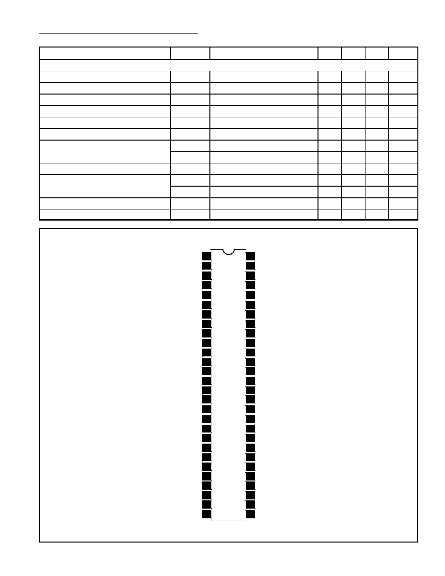
Pin Connection Diagram
X≠Ray
De≠Emphasis
Ext. Audio
R Output
Analog G Input
PIF GND
SIF Tank
V Sepa Filter
F≠BLK
APC Filter
PIF Input
AGC Filter
SIF GND
DC Restoration
VCXO
PIF Tank
1
2
3
4
Sound Outptu
Sound Output
RF AGC
5
6
7
8
PIF Input
56
55
54
53
Ext. Audio
Audio TV Input
52
Limiter Input
51
50
49
9
48
TV Det. Output
10
Loop Filter
11
47
46
Chroma Input
12
45
AFT
13
GND
44
Y Input
14
43
15
Analog R Input
42
Ext. Video
FBP Input
V. Ramp
ACL
TV Input
16
17
Analog B Input
18
19
20
G Output
41
AV/SW Output
40
Black Det
39
38
37
ABL
21
B Output
36
D. GND
22
23
35
34
H. AFC
24
33
H. Output
25
32
Sync Output
26
31
27
30
SDA
28
29
V. Output
NFB
SCL
PIF Tank
PIF V
CC
D. V
CC
H. V
CC

2.000 (50.9) Max
1
28
56
29
.551 (14.0)
.600 (15.24)
.165
(4.2)
.118 (3.0)
.070 (1.78)