NTE7160
Integrated Circuit
Video Switch
Features:
D
Standard Connection for VCR and Peri TV Sets
D
Input Clamping
D
Positive and Negative Video Outputs
Absolute Maximum Ratings:
Supply Voltage, V
S
16.5V
. . . . . . . . . . . . . . . . . . . . . . . . . . . . . . . . . . . . . . . . . . . . . . . . . . . . . . . . . . . . . . .
Operating Junction Temperature, T
J
+150
∞
C
. . . . . . . . . . . . . . . . . . . . . . . . . . . . . . . . . . . . . . . . . . . . . . .
Storage Temperature Range, T
stg
≠40
∞
to +125
∞
C
. . . . . . . . . . . . . . . . . . . . . . . . . . . . . . . . . . . . . . . . . .
Thermal Resistance, System≠to≠Ambient, R
thSA
70K/W
. . . . . . . . . . . . . . . . . . . . . . . . . . . . . . . . . . . .
Recommended Operating Conditions:
Parameter
Symbol
Test Conditions
Min
Typ
Max
Unit
Supply Voltage
V
S
10.0
≠
15.8
V
Video Bandwidth
B
video
≠
6
≠
MHz
Ambient Temperature Range
T
A
0
≠
70
∞
C
Electrical Characteristics: (V
S
= 13V, T
A
= +25
∞
C unless otherwise specified)
Parameter
Symbol
Test Conditions
Min
Typ
Max
Unit
Current Consumption
I
7
Pin2 Open
≠
23
≠
mA
Switch Input VCR, Recording
V
3/1
0
≠
1.2
Vdc
Switch Input VCR, Playback
V
3/1
3
≠
V
7
Vdc
Switch Input
I
3
V
3/1
= 15V
≠
≠
1
mA
Video Output Voltage, Positive
V
O5
pp
V
3
= 1.2V, V
8
pp = 3V
≠
3
≠
V
V
3
3V, V
4
pp = 1V
≠
3
≠
V
Sync Pulse Level
V
5/1
≠
2
≠
V
Output Current (To GND)
I
O5
≠
≠5
≠
mA
Output Current (To +)
I
O5
≠
2
≠
mA
Output Resistance
R
O5
≠
150
≠
Video Output Voltage, Negative
V
O6
pp
V
3
= 1.2V, V
8
pp = 3V
≠
3
≠
V
V
3
3V, V
4
pp = 1V
≠
3
≠
V
Sync Pulse Level
V
6/1
≠
V
7
≠2
≠
V
Electrical Characteristics (Cont'd): (V
S
= 13V, T
A
= +25
∞
C unless otherwise specified)
Parameter
Symbol
Test Conditions
Min
Typ
Max
Unit
Output Current (To GND)
I
O6
≠
≠5
≠
mA
Output Current (To +)
I
O6
≠
1
≠
mA
Output Resistance
R
O6
≠
150
≠
Video Output Voltage, Positive
V
O2
pp
V
8
pp = 3V, R
2/1
= 75
≠
1
≠
V
Sync Pulse Level
V
2/1
R
2/1
= 75
≠
1
≠
V
Output Current (To GND)
I
O2
≠
≠30
≠
mA
Output Current (To +)
I
O2
≠
2
≠
mA
Output Resistance
R
O2
≠
75
≠
Video Input Current
I
I8
V
8
pp = 3V
≠
≠
40
µ
A
I
I4
V
4
pp = 1V
≠
≠
20
µ
A
Video Gain
G
2/8
V
8
pp = 3V, R
2/1
= 75
≠
1/3
≠
G
5/8
V
8
pp = 3V, V
3
= 1.2V
≠
1
≠
G
6/8
V
8
pp = 3V, V
3
= 1.2V
≠
≠1
≠
G
5/4
V
4
pp = 1V, V
3
3V
≠
3
≠
G
6/4
V
4
pp = 1V, V
3
3V
≠
≠3
≠
Video Bandwidth
B
video
≠3dB
6
≠
≠
MHz
Crosstalk Rejection
Referred to V
5
pp = 3V,
f = 50Hz to 6MHz, V
3
= 1.2V,
V
4
pp = 1V
≠
50
≠
dB
+V
S
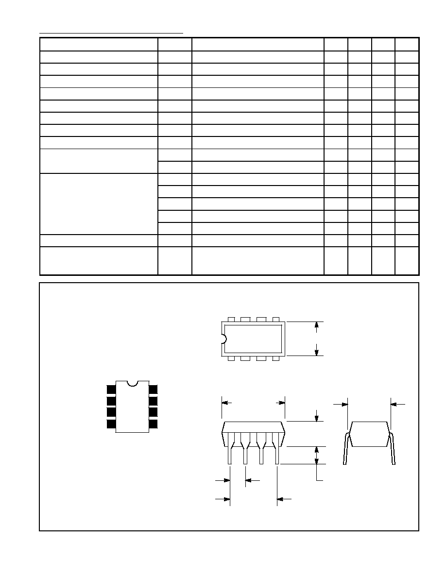
Pin Connection Diagram
8
5
.256 (6.52) Max
.393 (10.0)
Max
1
4
.300 (7.62)
.300 (7.62)
.150
(3.81)
.070 (1.77) Min
.100 (2.54)
Video (+)
Video Input
REC/PB Switch
1
2
3
4
GND
VCR Output
VCR Input
8
7
6
5
Video (≠)