NTE784
Integrated Circuit
Wide≠Band Power Amplifier
Description:
The NTE784 is a multistage, multipurpose, wide≠band power amplifier on a single monolithic silicon
chip. This device employs a highly versitile and stable direct≠coupled circuit configuration featuring
wide frequency range, high voltage and power gain, and high power output. These features plus in-
herent stability over a wide temperature range make the NTE784 extremely useful for a wide variety
of applications in military, industrial, and commercial equipment.
The NTE784 is particularly suited for service as a class B power amplifier and can provide a maximum
power output of 1W from a 12V DC supply with a typical power gain of 75dB.
Features:
D
High Power Output
D
Wide Frequency Range
D
High Power Gain
D
Single Power Supply for Class B Operation with Transformer
D
Built≠In Temperature Tracking Voltage Regulator Provides Stable Operation
Applications:
D
AF Power Amplifiers for Portable and Fixed Sound and Communications Systems
D
Servo≠Control Amplifier
D
Wide≠Band Linear Mixers
D
Video Power Amplifiers
D
Transmission≠Line Driver Amplifier (Balanced and Unbalanced)
D
Fan≠In and Fan≠Out Amplifiers for Computer Logic Circuits
D
Lamp≠Control Amplifiers
D
Motor≠Control Amplifiers
D
Power Multivibrators
D
Power Switches
Absolute Maximum Ratings:
Power Dissipation (Without Heatsink, T
A
= +25
∞
C), P
D
1W
. . . . . . . . . . . . . . . . . . . . . . . . . . . . . . . . . .
Derate Above 25
∞
C
6.7mW/
∞
C
. . . . . . . . . . . . . . . . . . . . . . . . . . . . . . . . . . . . . . . . . . . . . . . . . . . . .
Power Dissipation (With Heatsink, T
C
= +25
∞
C), P
D
2W
. . . . . . . . . . . . . . . . . . . . . . . . . . . . . . . . . . . . .
Derate Above 55
∞
C
16.7mW/
∞
C
. . . . . . . . . . . . . . . . . . . . . . . . . . . . . . . . . . . . . . . . . . . . . . . . . . . .
Operating Temperature Range, T
opr
≠55
∞
to +125
∞
C
. . . . . . . . . . . . . . . . . . . . . . . . . . . . . . . . . . . . . . . .
Storage Temperature Range, T
stg
≠65
∞
to +150
∞
C
. . . . . . . . . . . . . . . . . . . . . . . . . . . . . . . . . . . . . . . . . .
Maximum Thermal Resistance, Junction≠to≠Case, R
thJC
60
∞
C/W
. . . . . . . . . . . . . . . . . . . . . . . . . . . . .
Electrical Characteristics: (T
A
= +25
∞
C unless otherwise specified)
Parameter
Symbol
Test Conditions
Min
Typ
Max
Unit
Collector≠Emitter Breakdown Voltage
V
(BR)CER
(Q
6
& Q
7
) I
C
= 10mA
25
≠
≠
V
V
(BR)CEO
(Q
1
) I
C
= 0.1mA
10
≠
≠
V
Idle Currents
I
4
, I
7
(Q
6
& Q
7
) V
CC1
=9V, V
CC2
= 2V
≠
5.5
≠
mA
Peak Output Currents
I
4
, I
7
(Q
6
& Q
7
) V
CC1
=9V, V
CC2
= 2V
180
≠
≠
mA
Cutoff Currents
I
4
, I
7
(Q
6
& Q
7
) V
CC1
=9V, V
CC2
= 2V
≠
≠
1.0
mA
Differential Amplifier Current Drain
I
CC1
V
CC1
= 9V, V
CC2
= 9V
6.3
9.4
12.5
mA
Total Current Drain
I
CC1
+
I
CC2
V
CC1
= 9V, V
CC2
= 9V
14.5
21.5
30.0
mA
Differential Amplifier Input Pin Voltages
V
2
, V
3
V
CC1
= 9V, V
CC2
= 2V
≠
11.1
≠
V
Regulator Pin Voltage
V
11
V
CC1
= 9V, V
CC2
= 2V
≠
2.35
≠
V
Collector≠Emitter Cutoff Current
I
CEO
(Q) V
CC1
= 10V
≠
≠
100
µ
A
Emitter≠Base Cutoff Current
I
EBO
(Q) V
CC1
= 3V
≠
≠
0.1
µ
A
Collector≠Base Cutoff Current
I
CBO
(Q) V
CC1
= 3V
≠
≠
0.1
µ
A
Forward Current Transfer Ratio
h
FE1
(Q
1
) I
C
= 3mA, V
CC1
= 6V
30
75
≠
Bandwidth
BW
V
CC1
= 6V, V
CC2
= 6V, ≠3dB
≠
8
≠
MHz
Maximum Power Output
P
O(max)
V
CC1
= 6V, V
CC2
= 6V, R
CC
= 130
200
300
≠
mW
V
CC1
= 9V, V
CC2
= 9V, R
CC
= 130
400
550
≠
mW
V
CC1
= 9V, V
CC2
= 12V, R
CC
= 200
800
1000
≠
mW
Sensitivity
e
IN
V
CC1
= 9V, V
CC2
= 12V,
P
OUT
= 800mW, R
CC
= 200
≠
50
100
mV
Input Resistance
R
IN3
V
CC1
= 6V, V
CC2
= 6V, Pin3 to GND
≠
1000
≠
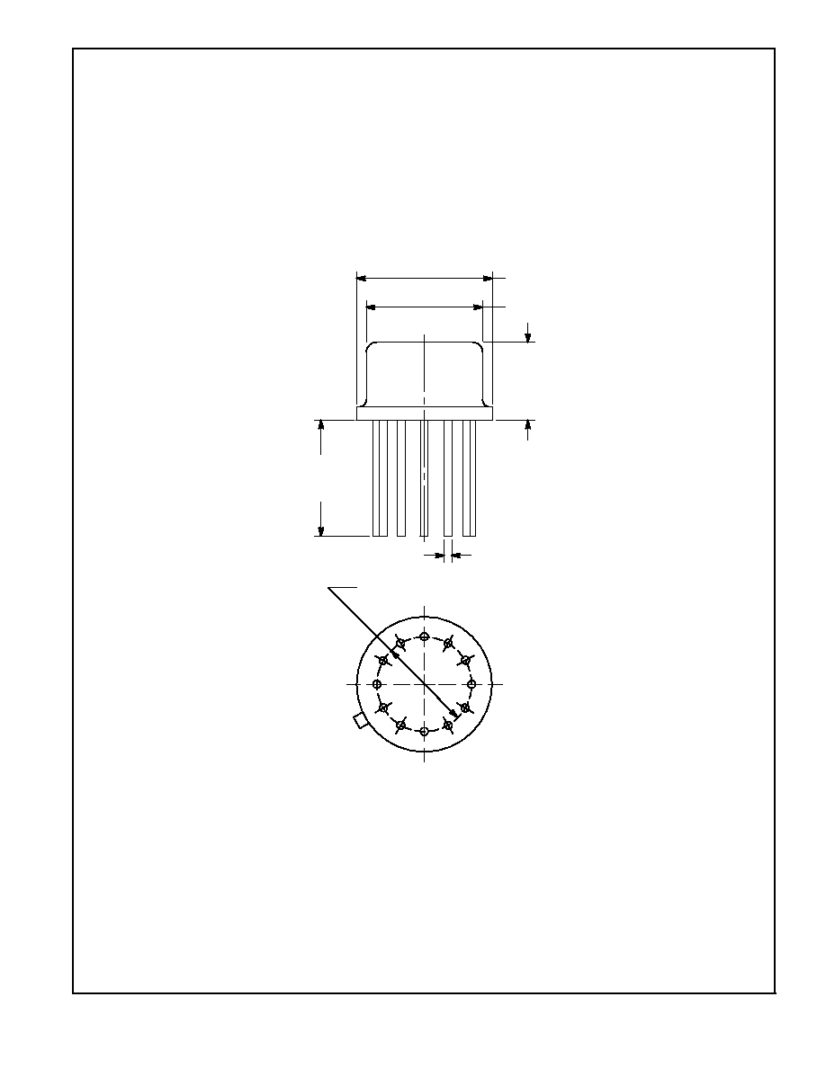
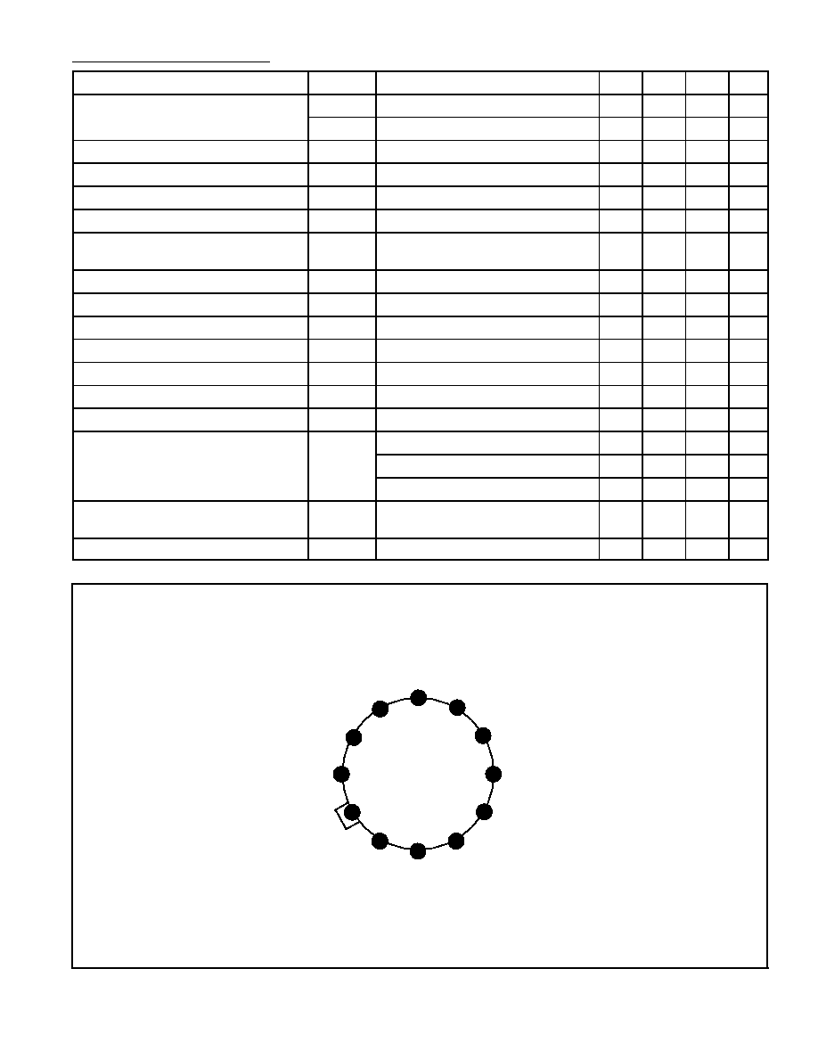
Pin Connection Diagram
(Top View)
12
11
10
6
5
4
3
9
6
1
8
7
1
2
GND
Buffer Amp Input
Emitter Output Q
2
2.1V Bias Point
Emitter Output Q
1
V
CC
Collector Output Q
2
Differential Amp Input "B"
Optional Bias Short to V
CC
Differential Amp Input "A"
Collector Output Q
1
Buffer Amp Output