NTE909 & NTE909D
Integrated Circuits
Operational Amplifier
Description:
These devices are monolithic operational amplifiers intended for general≠purpose applications. Op-
eration is completely specified over the range of voltages commonly used for these devices. The de-
sign, in addition to providing high gain, minimizes both offset voltages and bias currents. Further, the
class≠B output stage gives a large output capability with minimum power drain.
External components are used to frequency compensate the amplifier. Although the unity≠gain com-
pensation network specified will make the amplifiers unconditionally stable in all feedback configura-
tions, compensation can be tailored to optimize high≠frequency performance for any gain setting.
The fact that the amplifiers are built on a single silicon chip provides low offset and temperature drift
at minimum cost. It also ensures negligble drift due to temperature gradients in the vicinity of the am-
plifier.
Absolute Maximum Ratings:
Supply Voltage
±
18V
. . . . . . . . . . . . . . . . . . . . . . . . . . . . . . . . . . . . . . . . . . . . . . . . . . . . . . . . . . . . . . . . . . .
Power Dissipation (Note 1)
250mW
. . . . . . . . . . . . . . . . . . . . . . . . . . . . . . . . . . . . . . . . . . . . . . . . . . . . . .
Differential Input Voltage
±
10V
. . . . . . . . . . . . . . . . . . . . . . . . . . . . . . . . . . . . . . . . . . . . . . . . . . . . . . . . . . .
Input Voltage
±
10V
. . . . . . . . . . . . . . . . . . . . . . . . . . . . . . . . . . . . . . . . . . . . . . . . . . . . . . . . . . . . . . . . . . . . .
Output Short≠Circuit Duration (T
A
= +25
∞
C)
5 seconds
. . . . . . . . . . . . . . . . . . . . . . . . . . . . . . . . . . . . . .
Storage Temperature Range
≠65
∞
to +150
∞
C
. . . . . . . . . . . . . . . . . . . . . . . . . . . . . . . . . . . . . . . . . . . . . .
Operating Temperature Range
0
∞
to +70
∞
C
. . . . . . . . . . . . . . . . . . . . . . . . . . . . . . . . . . . . . . . . . . . . . . .
Lead Temperature (Soldering, 10 seconds)
+300
∞
C
. . . . . . . . . . . . . . . . . . . . . . . . . . . . . . . . . . . . . . . .
Note 1 For operating at elevated temperatures, the device must be derated based on a 100
∞
C maxi-
mum junction temperature and a thermal resistance 150
∞
C/W junction to ambient or 45
∞
C/W,
junction to case for the metal can package.
Electrical Characteristics: (0
∞
C
T
A
=
+70
∞
C,
±
9V
V
S
±
15V, C1 = 5000pF, R1 = 1.5k,
C2 = 200pF and R2 = 51
unless otherwise specified)
Parameter
Test Conditions
Min
Typ
Max
Unit
Input Offset Voltage
T
A
= +25
∞
C, R
S
10k
≠
2.0
7.5
mV
Input Bias Current
T
A
= +25
∞
C
≠
300
1500
nA
T
A
= T
MIN
≠
0.36
2.0
µ
A
Input Offset Current
T
A
= +25
∞
C
≠
100
500
nA
T
A
= T
MIN
≠
75
400
nA
T
A
= T
MAX
≠
125
750
nA
Electrical Characteristics (Cont'd): (0
∞
C
T
A
=
+70
∞
C,
±
9V
V
S
±
15V, C1 = 5000pF,
R1 = 1.5k, C2 = 200pF and R2 = 51
unless otherwise
specified)
Parameter
Test Conditions
Min
Typ
Max
Unit
Input Resistance
T
A
= +25
∞
C
50
250
≠
k
T
A
= T
MIN
50
250
≠
k
Output Resistance
T
A
= +25
∞
C
≠
150
≠
Supply Current
T
A
= +25
∞
C, V
S
=
±
15V
≠
2.6
6.6
mA
Transient Response Risetime
V
IN
= 20mV, C
L
100pF, T
A
= +25
∞
C
≠
0.3
1.0
µ
s
Transient Response Overshoot
≠
10
30
%
Slew Rate
T
A
= +25
∞
C
≠
0.25
≠
V/
µ
s
Average Temperature Coefficient
R
S
= 50
, T
A
= +25
∞
C to T
MAX
≠
6.0
≠
µ
V/
∞
C
of Input Offset Voltage
R
S
= 50
, T
A
= +25
∞
C to T
MIN
≠
12
≠
µ
V/
∞
C
Large Signal Voltage
V
S
=
±
15V, R
L
2k
, V
OUT
=
±
10V
15
45
≠
V/mV
Output Voltage Swing
V
S
=
±
15V, R
L
= 10k
±
12
±
14
≠
V
V
S
=
±
15V, R
L
= 2k
±
10
±
13
≠
V
Input Voltage Range
V
S
=
±
15V
±
8
±
10
≠
V
Common Mode Rejection Ratio
R
S
10k
65
90
≠
dB
Supply Voltage Rejection Ratio
R
S
10k
≠
25
200
µ
V/V
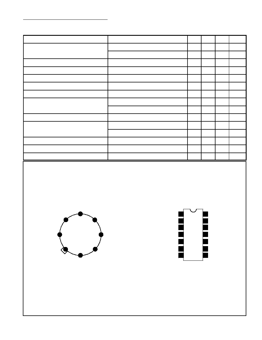
Pin Connection Diagram
NTE909
(Top View)
NTE909D
8
7
6
5
4
3
2
1
Input Freq Comp A
Invert Input
Non≠Invert Input
V (≠)
Output Freq Comp
Output
V (+)
Input Freq Comp B
Output Freq Comp
N.C.
1
2
3
4
N.C.
N.C.
Input Freq Comp A
Invert Input
5
Non≠Invert Input
6
V (≠)
7
N.C.
14
13
12
11
N.C.
Input Freq Comp B
V (+)
10
Output
9
8
N.C.