NTE918
NTE918M
NTE918SM
Integrated Circuit
High Speed Operational Amplifier
Description:
The NTE918, NTE918M, and the NTE918SM are precision high speed operational amplifier de-
signed for applications requiring wide bandwidth and high slew rate. These devices have internal uni-
ty gain frequency compensation. This considerably simplifies its application since no external compo-
nents are necessary for operation. However, unlike most internally compensated amplifiers, external
frequency compensation may be added for optimum performance. For inverting applications, feed-
forward compensation will boost the slew rate to over 150V/
µ
s and almost double the bandwidth.
Overcompensation can be used with the amplifier for greater stability when maximum bandwidth is
not needed. Further, a single capacitor can be added to reduce the 0.1% setting time to under 1
µ
s.
The high speed and fast setting time of these OP amps make them useful in A/D converters, oscilla-
tors, active filters, sample and hold circuits, or general purpose amplifiers. These devices are easy
to apply and offer an order of magnitude better AC performance than industry standards such as the
NTE909 and NTE909D.
Features:
D
15MHz Small Signal Bandwidth
D
Guaranteed 50V/
µ
s Slew Rate
D
Maximum Bias Current of 250nA
D
Operates from Supplies of
±
5V to
±
20V
D
Internal Frequency Compensation
D
Input and Output Overload Protected
D
Pin Compatible with General Purpose OP Amps
D
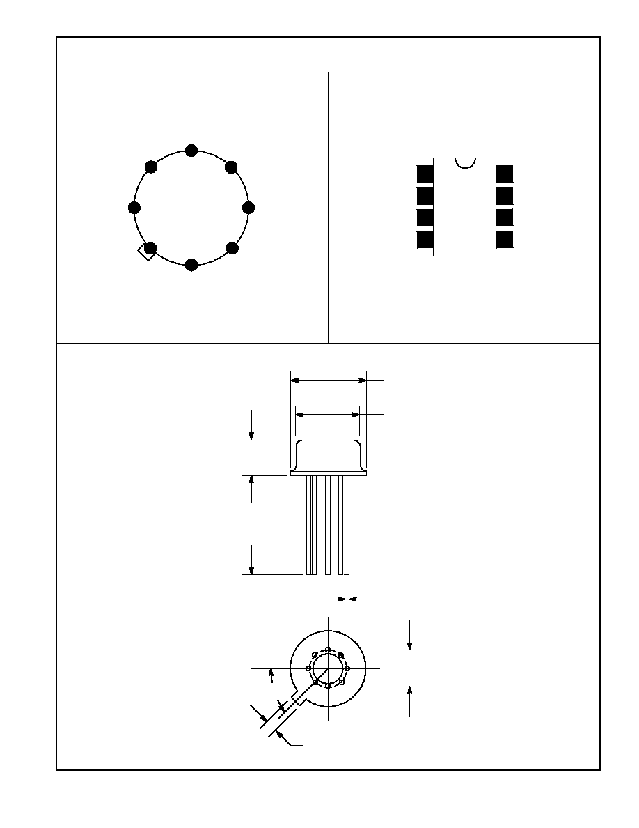
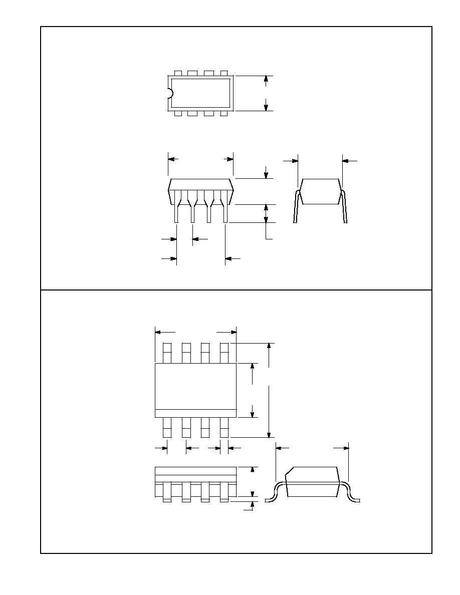
Available in 3 Different Case Styles:
8≠Lead Metal Can: NTE918
8≠Lead Mini DIP: NTE918M
8≠Lead SOIC (Surface Mount): NTE918SM

Absolute Maximum Ratings:
Power Supply Voltage, V
S
±
20V
. . . . . . . . . . . . . . . . . . . . . . . . . . . . . . . . . . . . . . . . . . . . . . . . . . . . . . . . . .
Power Dissipation (Note 1), P
D
500mW
. . . . . . . . . . . . . . . . . . . . . . . . . . . . . . . . . . . . . . . . . . . . . . . . . . .
Differential Input Current (Note 2), I
ID
±
10mA
. . . . . . . . . . . . . . . . . . . . . . . . . . . . . . . . . . . . . . . . . . . . . .
Input Voltage (Note 3), V
I
±
15V
. . . . . . . . . . . . . . . . . . . . . . . . . . . . . . . . . . . . . . . . . . . . . . . . . . . . . . . . . . .
Output Short≠Circuit Duration, t
S
Indefinite
. . . . . . . . . . . . . . . . . . . . . . . . . . . . . . . . . . . . . . . . . . . . . . . .
Operating Temperature Range, T
opr
0
∞
to +70
∞
C
. . . . . . . . . . . . . . . . . . . . . . . . . . . . . . . . . . . . . . . . . . .
Storage Temperature Range, T
stg
≠65
∞
to +150
∞
C
. . . . . . . . . . . . . . . . . . . . . . . . . . . . . . . . . . . . . . . . . .
Lead Temperature (During Soldering, 10sec), T
L
NTE918 (Metal Can)
+300
∞
C
. . . . . . . . . . . . . . . . . . . . . . . . . . . . . . . . . . . . . . . . . . . . . . . . . . . . . . .
NTE918M (Plastic DIP)
+260
∞
C
. . . . . . . . . . . . . . . . . . . . . . . . . . . . . . . . . . . . . . . . . . . . . . . . . . . .
NTE918SM (Surface Mount)
Vapor Phase (60sec)
+215
∞
C
. . . . . . . . . . . . . . . . . . . . . . . . . . . . . . . . . . . . . . . . . . . . . . . . . . .
Infrared (15sec)
+220
∞
C
. . . . . . . . . . . . . . . . . . . . . . . . . . . . . . . . . . . . . . . . . . . . . . . . . . . . . . . .
Note 1. The maximum junction temperature of these devices is +110
∞
C. For operating at elevated
temperatures, the NTE918 must be derated based on a thermal resistance of +150
∞
C/W,
junctio to ambient, or +45
∞
C/W, junction to case. The thermal resistance of the NTE918M
and the NTE918SM is +100
∞
C/W, junction to ambient.
Note 2. The inputs are shunted with back≠to≠back diodes for overvoltage protection. Therefore, ex-
cessive current will flow if a differential input voltage in excess of 1V is applied between the
inputs unless some limiting resistance is used.
Note 3. For supply voltages less than
±
15V, the absolute maximum input voltage is equal to the supply
voltage.
Electrical Characteristics: (
±
5V
V
S
±
20V, 0
∞
T
A
+70
∞
C, Note 4 unless otherwise specified)
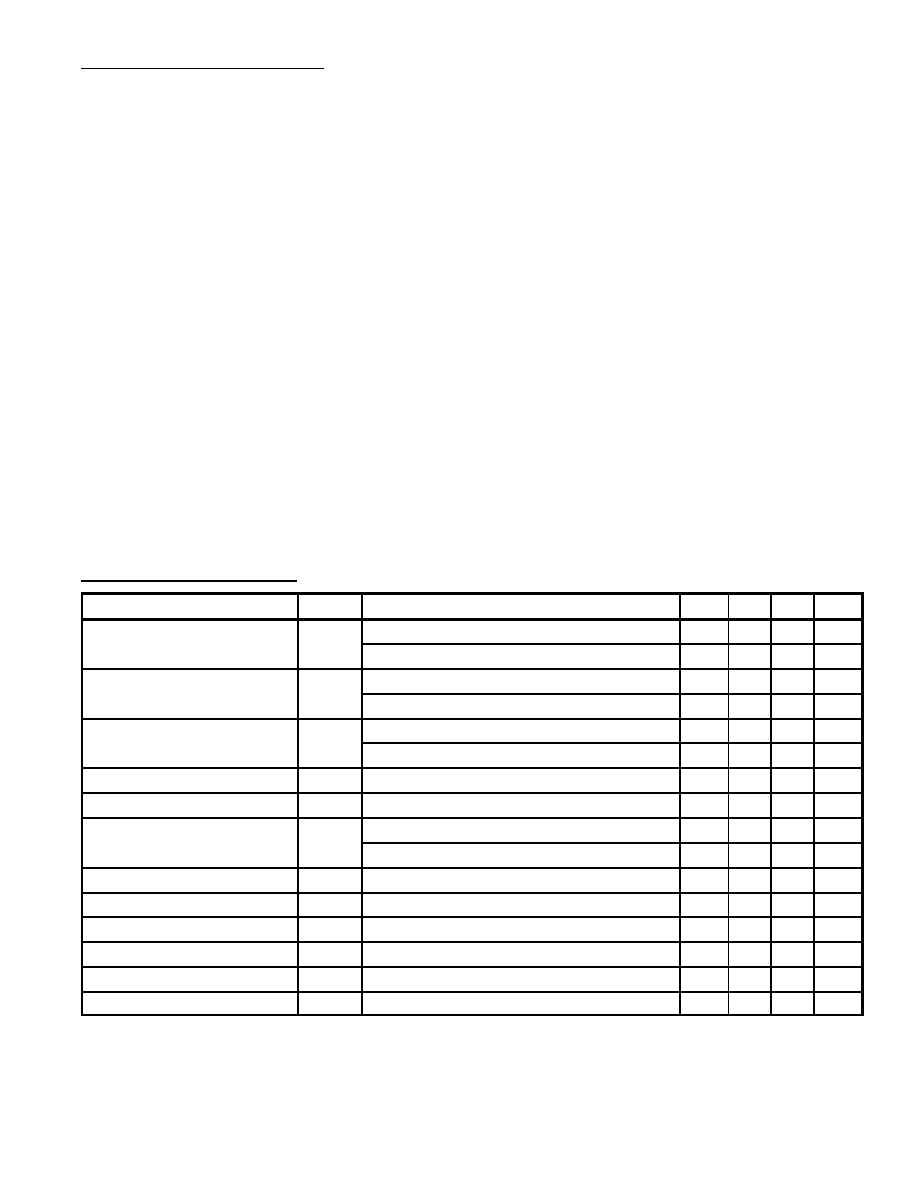
Parameter
Symbol
Test Conditions
Min
Typ
Max
Unit
Input Offset Voltage
V
IO
≠
≠
15
V
T
A
= +25
∞
C
≠
4
10
V
Input Offset Current
I
IO
≠
≠
300
nA
T
A
= +25
∞
C
≠
30
200
nA
Input Bias Current
I
IB
≠
≠
750
nA
T
A
= +25
∞
C
≠
150
500
nA
Input Resistance
r
i
T
A
= +25
∞
C
0.5
3.0
≠
M
Supply Current
I
CC
, I
EE
T
A
= +25
∞
C
≠
5
10
mA
Large Signal Voltage Gain
A
V
V
S
=
±
15V, V
OUT
=
±
10V, R
L
2k
20
≠
≠
V/mV
V
S
=
±
15V, V
OUT
=
±
10V, R
L
2k
, T
A
= +25
∞
C
25
200
≠
V/mV
Slew Rate
SR
V
S
=
±
15V, A
V
= 1, T
A
= +25
∞
C, Note 5
50
70
≠
V/
µ
s
Small Signal Bandwidth
BW
V
S
=
±
15V, T
A
= +25
∞
C
≠
15
≠
MHz
Output Voltage Swing
V
O
V
S
=
±
15V, R
L
= 2k
±
12
±
13
≠
V
Input Voltage Range
V
I
V
S
=
±
15V
±
11.5
≠
≠
V
Common≠Mode Rejection Ratio
CMRR
100
≠
≠
dB
Supply Voltage Rejection Ratio
PSRR
65
80
≠
dB
Note 4. Power supplies must be bypassed with 0.1
µ
F disc capacitors.
Note 5. Slew rate is tested with V
S
=
±
15V. These devices are in a unity≠gain non≠inverting configuration.
V
IN
is stepped from ≠7.5V to +7.5V and vice versa. The slew rates between ≠5V and +5V and
vice versa are tested and guaranteed to exceed 50V/
µ
s.


